AC POWER CONTROLLERS
DESCRIPTION:
The LS7310 - LS7313 are MOS integrated circuits specifically
designed for motor speed control applications in appliances
such as blenders, etc. I/Os (PLs) are provided for selecting/
indicating from one to ten power levels. The LS7310 and 7311
are designed for pushbutton control. The LS7312 and LS7313
are designed for touch control. (See Fig.4A and 4B)
INPUT/OUTPUT DESCRIPTION:
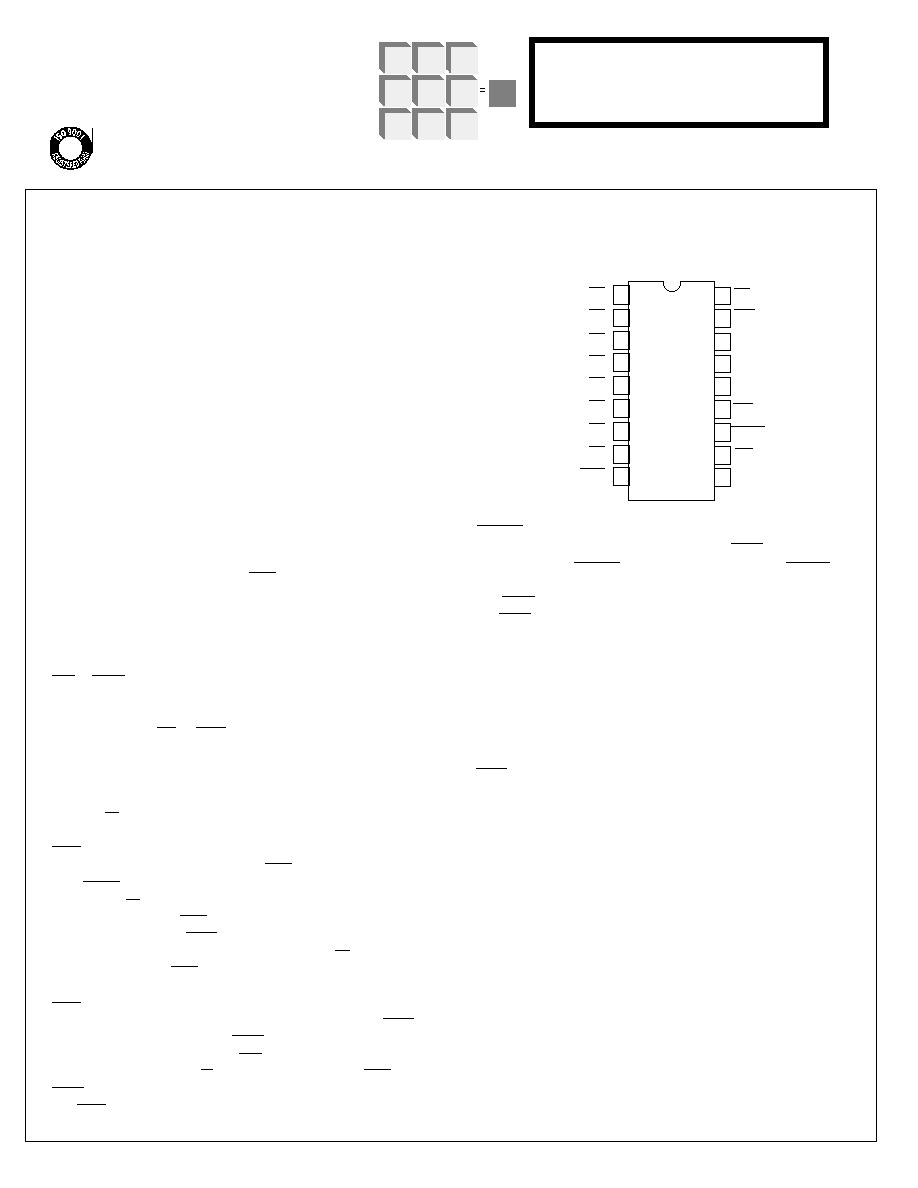
PL1 - PL10 (Pins 1 - 9, 18)
Ten inputs/outputs for selecting ten output phase angles (pow-
er levels). When no power level is selected (such as after sys-
tem power-up), PL1 - PL10 all act as inputs. When a power lev-
el is selected by applying a logic zero at one of these inputs for
T
H
time (See Dynamic Characteristics), the selected input
switches status to become an output in order to drive a display,
such as an LED. It switches back to the input state only when
another PL input is activated. (See Note 1)
RUN (Pin 13)
When a logic 0 is applied to the RUN input for T
H
time, the out-
put (TRIG) is turned on at a phase angle selected earlier by
one of the PL I/Os. If no power level was selected prior to the
application of the RUN input, the circuit remains unaffected.
Note that once the TRIG output has been enabled, its phase
angle can be altered by applying any other PL input without the
need to apply the RUN input again. (See Note 1)
OFF (Pin 11)
When a logic 0 is applied to this input for T
H
time, TRIG output
is turned off, if it was on. If TRIG was already off, the circuit re-
mains unaffected. Note that OFF input does not alter the power
level selected by a PL input. Following an OFF operation,
TRIG can be turned on at the previous phase angle by applying
the RUN input. (See Note 1)
1
2
3
4
5
6
7
8
9
10
11
12
13
14
15
16
17
18
PL2
PL3
PL4
PL5
PL6
PL7
PL8
PL9
P L 1 0
PL1
TRIG
Vss (+V)
SYNC
CAP
RUN
P U L S E
OFF
V
DD
(-V)
LSI
CONNECTION DIAGRAM - TOP VIEW
LS7310
FIGURE 1
January 2003
7310-012703-1
APPLICATIONS:
Universal and shaded-pole motor speed control for modern
appliance designs. Eliminates awkward mechanical switch
assemblies and multi-tapped motor windings.
PULSE (Pin 12)
A logic 0 applied to this input turns the TRIG output on for
as long as the PULSE input is maintained. The PULSE input
however, has no effect if no power level is in selection or if
the TRIG output has already been turned on by means of
the RUN input. (See Note 1)
SYNC (Pin 15)
Input for PLL reference frequency (50Hz/60Hz). All internal
clock frequencies are synchronized with the SYNC input.
CAP (Pin 14)
Input for component connection for the PLL filter capacitor.
TRIG (Pin 17)
This output is designed to drive a triac in series with the
load and control its firing angle with respect to the AC line.
The LS7310 and LS7312 provide a nominal 33µs output
pulse width. Since some motors have large inductive loads
producing a large phase delay between voltage and current,
a wider output pulse may be required. The LS7311 and
LS7313 produce a 1ms output pulse width. Otherwise,
these parts are identical to the LS7310 and LS7312,
respectively.
Vss (Pin 16)
Supply voltage positive terminal.
V
DD
(Pin 10)
Supply voltage negative terminal (ground).
NOTE 1: LS7310, LS7311 have an internal pullup resistor on this
input and LS7312, LS7313 do not. (See DC Electrical Character-
istics.)
LSI/CSI
LSI Computer Systems, Inc. 1235 Walt Whitman Road, Melville, NY 11747 (631) 271-0400 FAX (631) 271-0405
LS7310-7313
UL
Æ
A3800
FEATURES:
∑
10 I/Os to Select/Indicate up to ten Power Levels
∑
Inputs activated by Touch or Pushbutton Switch
∑
Output switches pure and precise AC Power to Load
∑
Operates with 50Hz/60Hz line frequency
∑
Rugged, latchup-free process technology
∑
+10V to +14V operation (Vss - V
DD
)
∑
LS7310 thru LS7313 (DIP);
LS7310-S thru LS7313-S (SOIC) - See Figure 1

7310-012703-2
TABLE 1. TRIG PHASE ANGLES (1)
PL INPUT TRIG ÿ LOAD POWER % (2
)
1
78∞
37
2
86∞
46
3
93∞
53
4
100∞
60
5
107∞
69
6
112∞
74
7
119∞
79
8
127∞
86
9
137∞
92
10
149∞
97
ÿ
T
W
FIGURE 3. TRIG PHASE ANGLE ÿ
SYNC
TRIG
(1)
The TRIG Phase Angles shown in TABLE 1 are referenced to the
SYNC input. In the Application Schematic shown in Figure 4A,
SYNC is delayed by 7∞ from the AC line. Therefore, actual Phase
Angles with respect to the AC line are 7∞ less than TABLE 1 values.
TABLE 1 values are mask programmable.
(2)
The percentage of Full Power delivered to a resistive load by the
Triac Switch.
FIGURE 4 VALUE TABLE
CONDITION C2(µF) C5(µF)
(1), (3), (5)
0.22
100
(1), (3), (6)
0.10
100
(1), (4), (5)
0.47
220
(1), (4), (6)
0.33
220
(2), (3), (5)
0.47
220
(2), (3), (6)
0.33
220
(2), (4), (5)
0.68
220
(2), (4), (6)
0.47
220
(1) 33µs TRIG pulse (LS7310, LS7312)
(2) 1ms TRIG pulse (LS7311, LS7313)
(3) No LEDs
(4) 5mA LEDs
(5) 115VAC, C2 = 200V
(6) 220VAC, C2 = 400V
FIGURE 4 NOTES
NOTE 1: Value for 5mA LEDs
NOTE 2: Use zener which produces 6.2V ±5% at 500µA or
less, i.e. P/N MZ4627
NOTE 3: R6-C6 Snubber Network may be required for large
inductive loads.
NOTE 4: Tie all unused touch inputs together and return to Vss
through 100k Ohm, 1/4W resistor.
D R I V E R
D R I V E R
+
-
13
12
11
18
9
C O N T R O L
LOGIC
D R I V E R
DIGITAL
C O M P A R A T O R
P O W E R
L E V E L
ROM
P H A S E
ANGLE
P O I N T E R
P H A S E - L O C K E D
L O O P
AND
C L O C K
G E N E R A T O R
L E V E L 1
L E V E L 1 0
15
14
+
-
+
-
+
-
+
-
+
-
V
SS
V
DD
V
SS
V
DD
TRIG
CAP
RUN
P U L S E
OFF
PL1
P L 1 0
17
FIGURE 2. LS7310-LS7313 BLOCK DIAGRAM
SYNC

M
P
N
L
MT2
G
MT1
C1
R1
R2
R9
C2
Z1
C5
D1
-
+
C4
C3
17
14
SYNC
CAP
15
10
13
12
11
18
9
16
Z2
R4
R5
V
SS
RUN
P U L S E
OFF
PL1
P L 1 0
L S 7 3 1 0 - L S 7 3 1 3
FIGURE 4A. APPLICATION SCHEMATIC FOR LS7310-LS7313
V
DD
R6
C6
TRIG
RUN
P U L S E
OFF
PL1
P L 1 0
AC
MAINS
SEE NOTE 3
T
R3
RUN
P U L S E
OFF
PL1
P L 1 0
FIGURE 4B. PUSHBUTTON INTERFACE FOR LS7310, LS7311
V
DD
R8
R8
R7
R8
R8
R7
R8
R8
R7
R8
R8
R7
R8
R8
R7
Vss
TP
TP
TP
TP
TP
P L 1 0
PL1
OFF
P U L S E
RUN
FIGURE 4C. TOUCH INTERFACE FOR LS7312, LS7313
S E E N O T E 4
C1 = 0.15µF, 200V (400V)
R1 = 82
C2 = See Figure 4 Value Table
R2 = 1.5M
C3 = 0.047µF
R3 = 10k
C4 = 470pF
R4 = 560
(See Note 1)
C5 = See Figure 4 Value Table
R5 = 10k
C6 = 0.47µF, 200V (400V)
R6 = 1.8k
, 1W (2W)
L = 100µH (200µH)
All resistors 1/4W, all capacitors 25V unless otherwise specified.
Indicates component change for 220VAC Mains.
*
*
*
R7 = 1M
to 5M
(Select For Sensitivity)
R8 = 2.7M
(4.7M
)
R9 = 100
Z1 = 13V ± 5%, 1W
Z2 = 6.2V, 1/4W (See Note 2)
D1 = 1N4148
T = Q4004L4 (Q5004L4) Typical
*
*
*
7310-012703-3
*

Input Pull-up Resistance:
For LS7310, LS7311
PL, OFF, RUN, PULSE
R
IN
50
100
200
k
-
Output Voltage:
TRIG, HI
V
OH
Vss
-
-
V
-
TRIG, LO
V
OL
-
Vss - 8
-
V
-
Output Current:
TRIG, Sink
I
OS
25
-
-
mA
Vss = +12V
V
OL
= Vss - 4V
PL Source
I
OPL
5
-
-
mA
V
OPL
= Vss - 1V
DYNAMIC CHARACTERISTICS:
SYMBOL
MIN
TYP
MAX
UNIT
CONDITION
SYNC frequency
f
S
40
-
70
Hz
-
PL, RUN, PULSE, OFF
T
H
50
-
infinite
ms
60Hz SYNC
Hold Time
T
H
60
-
infinite
ms
50Hz SYNC
TRIG Pulse Width
T
w
-
33
-
µs
60Hz SYNC
(LS7310, LS7312)
T
w
-
39
-
µs
50Hz SYNC
TRIG Pulse Width
T
w
-
1.0
-
ms
60Hz SYNC
(LS7311, LS7313)
T
w
-
1.2
-
ms
50Hz SYNC
MAXIMUM RATINGS:
PARAMETER
SYMBOL
VALUE
UNIT
DC Supply Voltage
Vss - V
DD
+20
V
Any Input Voltage
V
IN
Vss - 20 to Vss + 0.5
V
Storage Temperature
T
STG
-65 to +150
∞C
Operating Temperature
T
A
0 to +80
∞C
DC ELECTRICAL CHARACTERISTICS:
(TA = 25∞C, all voltages referenced to V
DD
)
SYMBOL
MIN
TYP
MAX
UNIT
CONDITION
Supply Voltage
V
SS
+10
+12
+14
V
-
Supply Current
I
DD
-
1.2
2
mA
Vss = 12V, outputs off
Input Voltage:
SYNC, LO
V
ISL
0
-
1/3Vss
V
-
SYNC, HI
V
ISH
2/3Vss
-
Vss
V
-
All other inputs, LO
V
IL
0
-
1/4Vss
V
-
All other inputs, HI
V
IH
1/2Vss
-
Vss
V
-
Input Current:
SYNC Input
I
H
-
-
110
µA
With Series 1.5M
Resistor to 115VAC
7310-012703-4
The information included herein is believed to be
accurate and reliable. However, LSI Computer Systems,
Inc. assumes no responsibilities for inaccuracies, nor for
any infringements of patent rights of others which may
result from its use.