 | –≠–ª–µ–∫—Ç—Ä–æ–Ω–Ω—ã–π –∫–æ–º–ø–æ–Ω–µ–Ω—Ç: LS7340 | –°–∫–∞—á–∞—Ç—å:  PDF PDF  ZIP ZIP |

AUTO SHUT-OFF AC POWER SWITCH
WITH PROGRAMMABLE TIMER
FEATURES:
∑ Phase-Lock Loop Synchronization allows use in
Wall Switch Applications.
∑ PLL accuracy delivers Pure AC Power.
∑ Timer programmable with external R-C.
∑ ON input switches AC Power On and starts Timer.
∑ OFF input switches AC Power Off.
∑ 50/60Hz Line Frequency.
∑ +12V to +18V Operation (V
SS
- V
DD
).
∑ LS7339, LS7340 ( DIP) - See Figure 1
LS7339-S, LS7340-S (SOIC)
APPLICATIONS:
∑ AUTO SHUT-OFF TIMER for appliances such as coffee pots,
curling irons, hair curlers, electric blankets, hand dryers.
∑ TIMED-ON WALL SWITCH for incandescent lighting and
heat lamps.
DESCRIPTION:
The LS7339 and LS7340 are monolithic MOS integrated circuits de-
signed to turn a triac On and Off in a Power Switch for AC loads. Ac-
tivation of the ON input will always turn the triac On and start a Timer.
The triac remains On for the duration of the Timer which is controlled
by an external R-C connected to the OSCILLATOR input. Activation
of the OFF input will always turn the triac Off. The two ICs differ only
in the width of the TRIG pulse used to trigger the triac. (See I/O De-
scription, Pin 4.)
In a typical application (Figure 5), the output of the LS7339 drives the
gate of a triac in series with the load. Because the LS7339 is ac-
curately synchronized to the line frequency with a phase-lock loop, the
power delivered by the triac to the load is pure AC, allowing use with
inductive loads such as motors and transformers.
There are two states through which the LS7339 can be stepped. The
states and their corresponding operating modes, phase angles, and
delivered power levels are shown in Table 1.
TABLE 1
(See Figures 2 and 3)
STATE 0
STATE 1
OPERATING MODE
OFF
Timed-On
PHASE ANGLE, ¯
No Output
159∞
% LOAD POWER (1)
0
99
(1) The percentage of full power delivered to a resistive load by the
triac switch.
If left in STATE 1, after a time-out period determined by the
frequency set at the OSC input (See I/O Description, Pin 6),
the circuit automatically steps to STATE 0. If the ON input tran-
sitions to logic 0 before completion of the time-out period in
STATE 1, the Timer is restarted, beginning a new time-out
June 2001
7339/40-032499-1
1
2
3
4
5
6
7
LSI
8
PIN ASSIGNMENT - TOP VIEW
FIGURE 1
ON
OFF
V
DD
(-V)
TRIG
V
SS
(+V)
S Y N C
CAP
OSC
LS7339/7340
LSI/CSI
LSI Computer Systems, Inc. 1235 Walt Whitman Road, Melville, NY 11747 (631) 271-0400 FAX (631) 271-0405
LS7339-7340
UL
Æ
A3800
OPERATING DESCRIPTION:
Upon power up, internal power-on-reset starts the LS7339 in STATE 0.
When the ON input transitions to logic 0, the circuit steps to STATE 1.
When the OFF input transitions to logic 0, the circuit steps to STATE 0.
When implemented as shown in the application example (Figure 5),
this is accomplished by the momentary switching of the appropriate in-
put to V
DD
through S1. STATE 1 is a quasi-stable state.
INPUT/OUTPUT DESCRIPTION:
ON (Pin 1) - See NOTE 1
A logic 0 applied to this input for a minimum of three SYNC cy-
cles, T
S1
(50ms for 60Hz, 60ms for 50Hz), turns TRIG On and
starts a Timer. Upon completion of the Time-out, T
D1
, TRIG
turns Off. While the Time-out is in progress a new transition to
logic 0 at this input for a minimum of three SYNC Cycles, T
S1
,
restarts the Timer. This input is designed for Touch or Switch
control. (See Figure 5.)
OFF (Pin 2) - See NOTE 2
A logic 0 applied to this input for a minimum of three SYNC cy-
cles, T
S1
, turns TRIG Off. This input is designed for Switch con-
trol only. (See Figure 5.)
V
DD
(Pin 3)
Supply voltage negative terminal.
TRIG (Pin 4)
TRIG is a negative going pulse occurring once every half cycle
of the SYNC input. Pulse width is 1ms (LS7339) or 33µs
(LS7340). The LS7339 wide pulse width may be required for in-
ductive loads. The LS7340 narrow pulse width allows use of a
smaller value of C2 power supply capacitor. (See Figure 5.)
V
SS
(Pin 5)
Supply voltage positive terminal.
OSC (Pin 6)
An R-C network connected to this input controls the frequency
of oscillation which determines the Time-out, T
D1
, in State 1. T
D1
is approximately 255RC. The Oscillator is active only in State 1.
Chip to chip Oscillation Tolerance is ±10% for fixed value of RC.
Tie Pin 6 to V
SS
if a Time-out is not desired. (See Figure 5.)
CAP (Pin 7)
The CAP input is for external component connection for the PLL fil-
ter capacitor. (See Figure 5.)
SYNC (Pin 8).
The AC Line Frequency (50/60Hz) is applied to this input. The
Phase-Lock Loop synchronizes all internal timings to the AC signal
at the SYNC input. (See Figure 5.)
NOTE 1: ON will function as described if OFF is at logic 1.
If OFF is held at logic 0, the transitions at ON will
not cause the output to turn On.
NOTE 2: OFF will function as described if ON is at logic 1.
If ON is held at logic 0, the transitions at OFF
will not cause the the output to turn Off.
Tw
Tw
¯
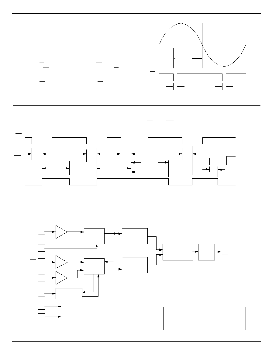
FIGURE 2. OUTPUT CONDUCTION ANGLE, ÿ
SYNC
TRIG
7339/40-032499-2
ON
OFF
ÿ
OFF
T
S1
T
D1
T
S1
T
S1
T
S1
T
S1
T
D1
<T
D1
OFF
OFF
159∞/STATE 1
159∞/STATE 1
159∞/STATE 1
T
D1 RESTART
OFF/STATE 0
FIGURE 3. PHASE ANGLE, ÿ, vs ON AND OFF
DIGITAL
COMPARATOR
¯
DECODE
SYNC
PHASE-ANGLE
POINTER
PHASE-
LOCK
LOOP
CONTROL
LOGIC
BUF
BUF
BUF
SYNC
CAP
ON
OFF
V
SS
V
DD
FIGURE 4. LS7339/7340 BLOCK DIAGRAM
TRIG
OSC/TIMER
OSC
(+V)
(-V)
DRIVER
4
8
7
1
2
6
5
3
The information included herein is believed to be
accurate and reliable. However, LSI Computer Systems,
Inc. assumes no responsibilities for inaccuracies, nor for
any infringements of patent rights of others which may
result from its use.
DC ELECTRICAL CHARACTERISTICS:
(T
A
= 25∞C, all voltages referenced to V
DD
)
PARAMETER
SYMBOL
MIN
TYP
MAX
UNIT
CONDITIONS
Supply Voltage
V
SS
+12
-
+18
V
-
Supply Current
I
SS
-
1.6
2.2
mA
V
SS
= +15V,
Output off
Input Voltages
SYNC Lo
V
IRL
0
-
V
SS
-9.5
V
-
SYNC Hi
V
IRH
V
SS
-5.5
-
V
SS
V
-
ON Lo
V
IOL
0
-
V
SS
-8
V
-
ON Hi
V
IOH
V
SS
-2
-
V
SS
V
-
OFF Lo
V
IVL
0
-
V
SS
-8
V
-
OFF Hi
V
IVH
V
SS
-2
-
V
SS
V
-
Input Current
SYNC, ON &
I
IH
-
-
110
uA
With Series 1.5M
OFF Hi
Resistor to 115VAC
SYNC, ON &
OFF Lo
I
IL
-
-
100
nA
-
TRIG Hi Voltage
V
OH
-
V
SS
-
V
-
TRIG Lo Voltage
V
OL
-
V
SS
-8
-
V
V
SS
= +15V
TRIG Sink Current
I
OS
25
-
-
mA
V
SS
= +15V,
V
OL
= V
SS
- 4V
TRANSIENT CHARACTERISTICS (See Fig. 2 and 3)
(All timings are based on Fs = 60Hz, unless otherwise specified.)
PARAMETER
SYMBOL
MIN
TYP
MAX
UNIT
SYNC Frequency
Fs
40
-
70
Hz
ON/OFF Sense Time
Ts
1
50
-
Infinite
ms
TRIG Pulse Width
(LS7339)
Tw
-
1.0
-
ms
(LS7340)
Tw
-
33
-
µs
STATE 1 Time-out
T
D1
-
255RC
-
s
ABSOLUTE MAXIMUM RATINGS:
PARAMETER
SYMBOL
VALUE
UNIT
DC supply voltage
V
SS
- V
DD
+20
V
Any input voltage
V
IN
V
SS
-20 to V
SS
+ .5
V
Operating temperature
T
A
0 to +85
∞C
Storage temperature
T
STG
-65 to +150
∞C
7339/40-032499-3
TABLE 2. COMPONENT FUNCTIONAL DESCRIPTION FOR FIGURE 5
COMPONENTS FUNCTIONAL DESCRIPTION
Z1, D1, R1, C2, C3
DC Power Supply.
R2, C4
Current limit and filter AC for SYNC input.
C1, L1
RFI filtering for AC Mains.
C5
PLL filter capacitor.
R5
Current limiting and isolation betweenIC output and Triac Gate.
R6, R7, C6
Oscillator R-C network.
Potentiometer R6 required only if providing user adjustment of Time-out, TD1.
R3, R4
Pullup resistors to establish normally inactive condition of ON and OFF inputs.
S1
Momentary Double Throw Switch used to activate appropriate input.
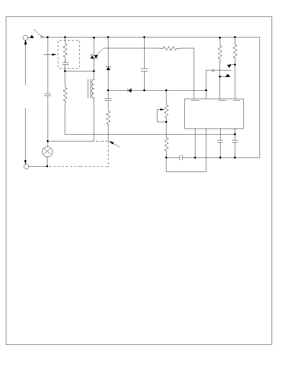
P
AC
MAINS
N
LOAD
C1
T1
L1
R1
A
B
R4
C3
D1
5
6
7
8
4
3
2
1
C5
C4
TRIG V
DD
OFF
ON
V
SS
OSC
CAP SYNC
+
L S 7 3 3 9
FIGURE 5. A TYPICAL AUTO SHUT-OFF AC POWER SWITCH
G
MT2
MT1
Z1
-
R5
C7
R8
C6
S E E
N O T E 1
S E E
N O T E 2
R7
R6
R2
R3
C2
ON
OFF
S1
-
+
115VAC
220VAC
115VAC 220VAC
(1)(3) R1 150
, 1W
360
, 2W (1)(2)C3 100µF
100µF
(2)(4) R1 82
82
(3)(4)C3 47µF
47µF
R2 1.5M
1.5M
C4 470pF
470pF
R3 100k
100k
C5 0.047µF
0.047µF
R4 100k
100k
C6 (6)
(6)
R5 100
100
C7 0.1µF, 200V 0.1µF, 400V
R6 (5)(6)
(5)(6)
Z1
15V, 1/2W
15V, 1/2W
R7 (5)(6)
(5)(6)
D1 1N4148
1N4148
R8 1.8k
, 1W
1.8k
, 2W L1 100µH 200µH
C1 0.15µF, 200V 0.15µF, 400V (7)T1 Q4008L4
Q5004L4
(1) C2 1.0µF, 200V 0.47µF, 400V
(2) C2 0.47µF, 200V 0.22µF, 400V
(3) C2 0.33µF, 200V 0.22µF, 400V
(4) C2 0.22µF, 200V 0.1µF, 400V
(1) LS7339, Connection A
(2) LS7339, Connection B
(3) LS7340, Connection A
(4) LS7340, Connection B
(5) 100k
(R6 + R7)
10M
(6) (R6 + R7)C6
5ms
(7) Typical
All Resistors 1/4W, all Capacitors 25V unless otherwise specified
NOTES: 1. Use Connection A when Neutral is not available. Use Connection B when Neutral is available.
2. Snubber Network C7, R8 may be required for some inductive loads.
3. See Table 2 for Component Functional Description.
7339-060201-4
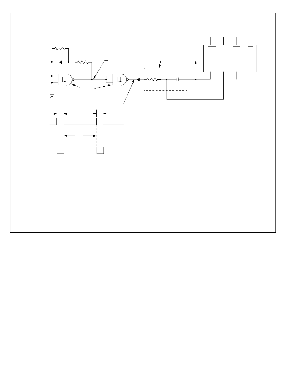
FIGURE 6. PRODUCING VERY LONG TIME-OUTS BY PULSE MODULATING THE OSCILLATOR
Oscillator
Components
R2
R1
C D 4 0 9 3
C 1 = 0 . 1 µ F
-V
R3
C2
-
+
4
3
TRIG
V
DD
V
SS
OSC
5
6
2
1
8
7
OFF
ON
CAP
SYNC
T1
T2
Waveform A
L S 7 3 3 9
T1
R1 C1
T2
(R1 + R2)C1
DESCRIPTION:
EXAMPLE:
D1
T1
Period = T1 + T2
Pulse Duty Cycle = T1/Period
-V
Waveform B (Pulse Modulator)
Inverse of Pulse Duty Cycle = Period/T1 = 1 +T2/T1 = 2 + R2/R1
Waveform A
Waveform B
+V
D2
The Oscillator resistor is normally returned to the negative terminal of the DC Supply. If this resistor is returned to
a negative-going pulse instead, the Oscillator R-C becomes effectively multiplied by the inverse of the Pulse Duty
Cycle, because the Oscillator R-C can charge only while the pulse is present. (Pulse Modulation)
In Figure 6, the Oscillator R is R3, the Oscillator C is C2 and the Pulse Modulator is Waveform B through
isolation diode D2. The Multiplier, M = 2 + R2/R1 (the inverse of the Pulse Duty Cycle).
R3 = 5.1M
, C2 = 1.0µF, Pulse Modulator = Waveform B and desired T
D1
= 8 hours = 28,800 sec.
Since T
D1
= 255 x M x R3 x C2, M calculates to be 22 for the selected Oscillator Components.
With M = 22, R2/R1 = 20. If R2 = 3M
, R1 = 150k
.
7339-060201-5