
YGV619 CATALOG
CATALOG No.: LSI-4GV619A1
2001.01
YGV619
AVDP6
Advanced Video Display Processor 6
s
Outline
YGV619 is a VDP (Video Display Processor) adopting OSD display control system
which is best suited to the
data broadcasting. The digital image interface of this device for connection with MPEG decoder has been
improved. The use of this device allows screen composition that is suited to mobile information terminals, car
navigation system, etc. Scan timing conforming to the display standard of digital TVs can be made.
Two built-in PLL circuits allows to realize superimposition of external image signal on original image signal,
and to produce clock best suited to SDRAM that is adopted as external video memory.
s
Features
q
Display planes: External digital image is overlaid with OSD images composed of regions.
Up to four planes, which are individually composed of back drop plane (plane on which external images are
inputted)
+ region, are available.
q
OSD image format:
8bit/dot palette mode, and 16 bit RGB or YCbCr format can be selected.
YCbCr conforms to the conversion method of ITU601.
Color palette (256 colors in 16777 k colors) can be specified by region.
q
Digital image input format:
� 18bitR6G6B6
(Max. dot clock frequency:
80 MHz)
� 16bitYCbCr422
(Max. dot clock frequency:
80 MHz)
� 8bitITU656
(Dot clock frequency
27 MHz)
q
Digital image output format:
� R6G6B6 + 2 bit AT
� 18bitYCbCr444 + 2 bit AT
� 16bitYCbCr422 + 2 bit AT
� 8bitITU656 + 2 bit AT + 6 bit
blending coefficient
q
Max. OSD resolution: 960 dots
�
1080 lines
(However, max. resolution of overlaid external image is 1920
�1080 lines)
q
Applicable digital TV image format:
� 525i
� 525p
� 1125i
q
Video capture function:
� Draws external image input on the frame memory in real time.
� Can convert resolution.
� Provided with progressive scanning conversion
YGV619
2
q
Priority of display planes
Regular priority: Plane D > Plane C > Plane B > Plane A > Back drop plane
The priority can be changed by region.
q
blending function (64 intensity level)
Blending weight can be set by dot.
q
Flicker cancel filter is built in.
Enabling / disabling flicker cancel function can be set by region.
q
8 bit DACs are built in for R, G and B individually. (Max. operating frequency: 80 MHz)
q
Two PLLs are built in. (1: Generates SDRAM clock and system clock 2: Generates dot clock)
q
Display monitor control
� Display resolution and scanning frequency can be set optionally.
This function is compatible with progressive scanning and interlaced scanning modes.
NTSC subcarrier output
q
SDRAM can be added externally as VRAM (SDRAM generation clock frequency: Max. 80 MHz.)
�16 bit bus
512k words � 16 bits � 2 banks � 1 pc.
(capacity:
2M bytes)
1M words � 16 bits � 4 banks � 1 pc.
(capacity:
8M bytes)
2M words � 16 bits � 2 banks � 1 pc.
(capacity: 8M bytes)
�32 bit bus
512k words � 16 bits � 2 banks � 2 pcs.
(capacity: 4M bytes)
512k words � 32 bits � 4 banks � 1 pc.
(capacity: 8M bytes)
1M words � 16 bits � 4 banks � 2 pcs.
(capacity: 16M bytes)
2M words � 16 bits � 2 banks � 2 pcs.
(capacity: 16M bytes)
q
CPU interface
Compatible with 16/32 bit CPU. Various built-in tables can be mapped on CPU space.
Compatible with little endian and big endian
q
Package:
240SQFP (YGV619-S)
q
Operating temperature range: -45 to +85
�
C
q
Power supply: 3.3V, single power supply
Supplementary information:
For YGV619, Application Manual that details the specifications of the device and the evaluation board
(MSY619DB01) are available in addition to this brochure.
The evaluation board is equipped with an SDRAM of 16 MB as a video memory. A high performance system
can be realized when it is used with Hitachi's CPU board, Super H Solution Engine.
The device driver provided by Yamaha and attached to the evaluation
board consists of the main body of the driver and API related layers,
allowing the user to build it into the system easily according to the
environment.
For the details of these products, inquire of the sales agents or our
business offices.
For CPU board, inquire of: Hitachi ULSI Systems Co., Ltd.
Tel:+81-42-351-6600

YGV619
3
s
Block Diagram
A23-2
D31-0
CPU
INTERFACE
CSREG
RD
A1
/
WR3
WR2-0
WAIT
SDRAM
INTERFACE
DRAWING
PROCESSOR
UNIT
PIXEL
DATA
CONTROLLER
CRT
CONTROLLER
DAC
HSYNC
CSYNC
VSIN
HSIN
SDQ31-0
SA12-0
SBA1-0
SDCLK
SCS
RAS
CAS
WE
DQM3-0
CSMEM
INT
RESET
DCKIN
DCKOUT
DRI[5:0]
DGI[5:0]
DBI[5:0]
DRO[5:0]
DGO[5:0]
DBO[5:0]
AT1-0
R,
G,
B
VIDEO
CAPTURE
CONTROLLER
GCKIN
GCKOUT
READY
SYCKIN
SYCKOUT
FSC
DREQ
AVDP6 performs parallel processing
including operation of writing display data into video memory (SDRAM)
connected on the local bus (drawing function) and operation of sequentially reading bit map image stored in the
video memory in accordance with monitor scanning (display function).
Drawing function:
This function transfers bit map image data configured on the external memory of CPU to video memory. For the
transfer of the data, a method that maps the video memory as external memory managed by CPU and performs the
transfer as the transfer between external memories of CPU,
or a method that uses internal drawing processor of
AVDP6 to configure the display image on the video memory can be used.
Display function:
This function displays the bit map image stored in the video memory in accordance with the display parameters
that are stored in the internal registers of AVDP6 and the video memory.
Basically, AVDP6 automatically sends out
display data and refreshes SDRAM once initial setting for internal registers are completed. When performing
dynamic processing such as scroll, the processing that synchronizes with the scanning of AVDP6 can be performed
easily by using internal flag polling of AVDP6 or interrupt function.
YGV619
4
s
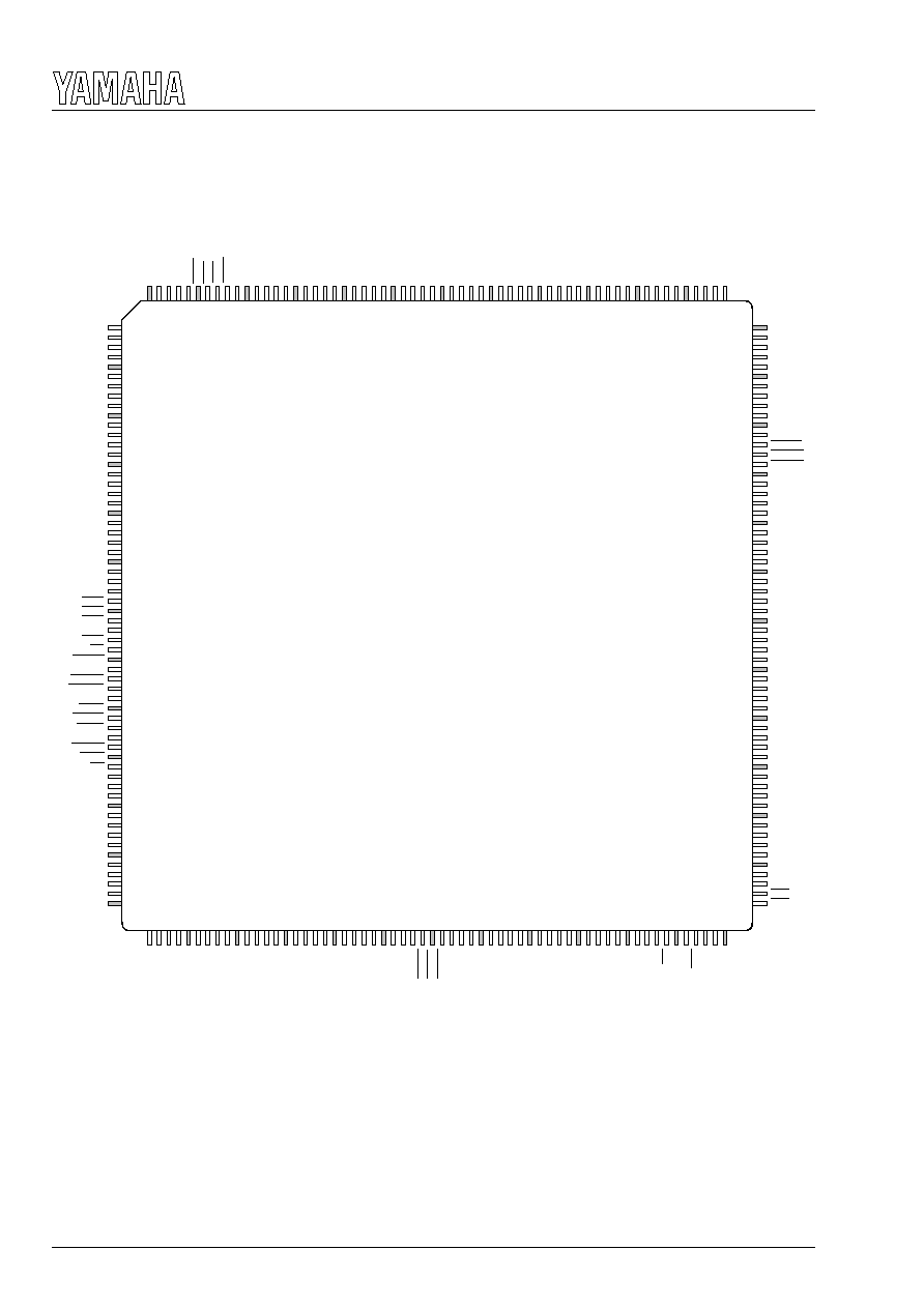
Pin Assignment
Top view
A V S S 1
A 2 3
A 2 1
A 1 9
A V D D 1
A 2 2
A 2 0
A 1 8
A 1 7
A 1 5
V S S
V D D
A 1 6
A 1 3
A 1 1
A 9
A 1 4
A 1 2
A 1 0
A 8
A 6
V S S
A 7
A 5
A 4
A 2
W R 2
V D D
A 3
A 1
/
W R 3
V S S
R D
V D D
W R 1
W R 0
R E S E T
C S M E M
L E N D
D R E Q
C S R E G
L W D
S Y C K S
R E A D Y
V S S
W A I T
I N T
V D D
D 2 9
D 2 7
D 3 1
D 3 0
D 2 8
D 2 5
V S S
D 2 2
D 2 6
D 2 4
D 2 3
V D D
D 2 1
1
2
3
4
5
6
7
8
9
10
11
12
13
14
15
16
17
18
19
20
21
22
23
24
25
26
27
28
29
30
31
32
33
34
35
36
37
38
39
40
41
42
43
44
45
46
47
48
49
50
51
52
53
54
55
56
57
58
59
60
D20
D18
D16
D15
D19
D17
VSS
D13
D11
D10
D14
D12
VDD
D8
D7
D5
D9
VSS
D6
D3
D1
D4
D2
D0
SYCKOUT
VDD
TEST1
VSS
SYCKIN
TEST2
SDQ0
SDQ1
SDQ14
TEST0
SDQ15
VSS
SDQ13
VDD
VSS
SDQ2
SDQ3
SDQ12
SDQ11
SDQ4
SDQ5
SDQ10
VSS
SDQ7
DQM0
SDQ6
SDQ9
SDQ8
WE
DQM1
SDCLK
VDD
VSS
CAS
AVDD2
AVSS2
61
62
63
64
65
66
67
68
69
70
71
72
73
74
75
76
77
78
79
80
81
82
83
84
85
86
87
88
89
90
91
92
93
94
95
96
97
98
99
100
101
102
103
104
105
106
107
108
109
110
111
112
113
114
115
116
117
118
119
120
DRO0
DGO4
DGO3
DGO1
DGO5
VSS
DGO2
DBO5
DBO4
VDD
DGO0
VSS
DBO3
DBO1
VSS
B
DBO2
DBO0
AVSS4
G
R
AVSS4
AVSS4
AVSS4
AVDD4
AVSS3
DRI4
REXT
AVDD3
DRI5
DRI2
DRI1
DRI0
DRI3
VSS
VDD
DGI4
DGI2
DGI0
DGI5
DGI3
DGI1
DBI4
DBI5
VSS
DBI3
DBI1
DBI0
GCKS
DBI2
VDD
GCKIN
VSIN
TCK80
DCKOUT
HSIN
TCKS
VSS
VDD
DCKIN
181
182
183
184
185
186
187
188
189
190
191
192
193
194
195
196
197
198
199
200
201
202
203
204
205
206
207
208
209
210
211
212
213
214
215
216
217
218
219
220
221
222
223
224
225
226
227
228
229
230
231
232
233
234
235
236
237
238
239
240
121
122
123
124
125
126
127
128
129
130
131
132
133
134
135
136
137
138
139
140
141
142
143
144
145
146
147
148
149
150
151
152
153
154
155
156
157
158
159
160
161
162
163
164
165
166
167
168
169
170
171
172
173
174
175
176
177
178
179
180
R A S
S B A 1
V S S
V D D
S C S
S A 1 1
S B A 0
S A 9
S A 8
S A 1
S A 1 2
S A 1 0
S A 0
V S S
S A 2
V D D
S A 6
S A 7
S A 5
S A 4
D Q M 3
S A 3
D Q M 2
V S S
S D Q 3 1
S D Q 3 0
V S S
S D Q 1 6
S D Q 1 7
S D Q 1 8
V D D
S D Q 2 8
S D Q 2 7
S D Q 2 9
S D Q 1 9
S D Q 2 0
S D Q 2 1
S D Q 2 2
S D Q 2 3
V S S
S D Q 2 6
S D Q 2 5
S D Q 2 4
V S S
V D D
C S Y N C
B L A N K
A T 1
A T 0
H S Y N C
F S C
V S S
D R O 5
D R O 3
D R O 2
G C K O U T
D R O 4
V S S
V D D
D R O 1

YGV619
5
s
Pin Functions
< CPU INTERFACE >
l
D31-0
(
(
(
(I/O: Pull Up))))
CPU data bus. D31-16 pins are not used for 16 bit CPU (LWD=0).
These pins are provided with a pull-up resistor.
Unused pins are to be open.
l
A23-8
(
(
(
(I: Pull Up)))),
A7-2
(
(
(
(I))))
CPU address bus. When accessing
CSREG space, signals inputted to A23-8 pins are ignored without regarding to the
bus width of CPU. Internal registers are selected depending on the state of signals inputted to A7-2 for 32 bit CPU or A7-
2 and
A1
/
WR3 pin for 16 bit CPU. Systems that control AVDP6 only with CSREG do not use this address bus.
However, A23-8 pins must be open because they are provided with pull-up resistor. All the addresses are valid when
accessing
CSMEM space.
l
CSREG
(
(
(
(I))))
Chip select signal input to REG space. Internal registers of AVDP6 are accessed by a using write / read pulse that is
inputted when the chip select signal is active.
When this signal is low, inputs to A23-8 pins are ignored.
l
CSMEM
(
(
(
(I))))
CSMEM is made active when directly mapping the video memory connected to local bus of AVDP6 on the memory
space of CPU. The video memory managed by AVDP6 is directly accessed using write / read pulse that is inputted with
this chip select signal is active. The video memory can be accessed from REG space without using this pin, however, high
level signal must be inputted to
CSMEM in this case.
l
LWD
(I: Pull Up)
Selects a CPU data bus width. When high level signal is inputted to this pin, AVDP6 operates as CPU 32 bit device, or
when low level signal is inputted to this pin, AVDP6 operates as CPU 16 bit device.
l
A1
/
WR3 , WR2-0
(
(
(
(I))))
Controls write access to AVDP6 when chip select input signal is active.
A1
/
WR3 control D31-24, WR2 controls
D23-16,
WR1 controls D15-8, and WR0 controls D7-0.
For 16 bit CPU,
A1
/
WR3 function as A1 of CPU address. WR2 is not used, and thus must be open because the pin is
provided with a pull-up resistor.
l
RD
(
(
(
(I))))
Controls read access to AVDP6 when chip select input signal is active. D31-0 pins are in output state while this signal
and chip select signals are active.
For 16 bit CPU, only D15-0 pins are in output state and D31-16 pins are in input states
at all times.
l
WAIT
(
(
(
(O: Pull Up, 3-state output))))
Data wait signal output to CPU. When
CSREG pin or CSMEM pin (hereafter called "CS pin") is active, the WAIT
signal is asserted once for
RD or A1
/
WR3 and WR2-0 signals, and then negated when AVDP6 becomes accessible.
This pin becomes high impedance state when
CS pin is not active, and outputs high level signal when CS pin is active
and
RD or A1
/
WR3 and WR2-0 pins are not active. Use this pin or READY depending on the type of CPU.
l
READY
(
(
(
(O: Pull Up, 3-state output))))
Data ready signal output to CPU. When AVDP6 becomes accessible, this signal is asserted. This pin becomes
high
impedance state when
CS pin is not active, outputs high level signal when CS pin is active and RD or
A1
/
WR3,
WR2-0 pins are not active. Use this pin or WAIT depending on the type of CPU.
l
INT
(
(
(
(O))))
Interrupt request signal output to CPU. This pin becomes active when internal state of AVDP6 coincides with the
setting conditions of the registers, and is reset when internal registers of AVDP6 are accessed.