 | –≠–ª–µ–∫—Ç—Ä–æ–Ω–Ω—ã–π –∫–æ–º–ø–æ–Ω–µ–Ω—Ç: 80C200 | –°–∫–∞—á–∞—Ç—å:  PDF PDF  ZIP ZIP |
80C200
4-1
1
MD400179/≠
98203
80C200
Full Duplex CMOS Ethernet
10/100 Mega Bit/Sec Data Link Controller
Features
s
Low Power CMOS Technology
s
10/100 MBit Ethernet Controller Optimized for
Switching Hub, Multiport Bridge/Router, &
Server Applications
s
Meets ANSI/IEEE 802.3 and ISO 8802-3 Standards
for Ethernet (10Base-5) Thin Net (10Base-2)
(10Base-T) and the Proposed 100Base-T4,
100Base-TX Standards
s
Programmable MII Ethernet Interface for 10/100
MBit/sec Applications
s
Programmability of Double Word Threshold
Count for Space Available/Data Available Ready
Condition for Transmit/Receive FIFOs
s
Auto Retransmit Upon Collision Sense
s
Preamble Generation and Removal
s
Automatic 32-Bit FCS (CRC) Generation and
Checking
s
Collision Handling, Transmission Deferral and
Retransmission with Automatic Jam and
Backoff Functions
s
Error Interrupt and Status Generation
s
Selectable Little Endian/Big Endian Transmit Byte
Ordering for FIFO Interface for Intel/Motorola
Compatibility
s
Single 5 V
±
5% Power Supply
s
Standard CPU and Peripheral Interface
Control Signals
s
128/128 Byte Independent Transmit/Receive FIFOs
with 32 Bit Data Path Interface
- 1 G Bits/sec (133 M Bytes/sec) Peak Data Rate
in 32 Bit Mode.
s
Loopback Capability for Diagnostics
s
32 Bit FIFO Data Path
s
Inputs and Outputs TTL Compatible
s
The Following Additional Features can be
Programmed for the 80C200
- 64 bit Multicast Filter
- Reports Status of "SQE" During Transmits
- Transmit No CRC Mode
- Transmit No Preamble Mode
- Transmit Packet Autopadding Mode
- Receive CRC Mode
- Disable Self-Receive on Transmit Mode
- Disable Further Transmissions when Both
Transmit Status Registers are Full
Hurricane is a trademark of SEEQ Technology Inc.
- Disable Loading the Transmit Status for
Successfully Transmitted Packets
- Disable the Receive Interrupts Independent
of the Receive Command Register Setting
- Successful Packet Transmit Completion
Feature
s
Full Duplex Operation
- Provides 20/200 Mbps Bandwidthfor
Switched Networks
s
Transmit Status on a Per Packet Basis Reports the
Following
- Occurrence of a Transmit FIFO Underflow
- Transmit Collision Occurrence
- 16 Collision Occurrence
- Carrier Sense Error During Transmission
- 10/100 Mbit/sec Transmit Clock Detect
- Late Collision Occurrence
- Transmission Successful
- Transmission Deferred
s
Management Counters for
- Alignment Errors
- FCS Errors
- Runt Receive Frames
- Short Receive Events
- Oversized Receive Packets
- Transmit Collisions
- Receive Collisions
- Very Long Transmit Events
- Excessive Transmit Deferral
- Late Transmit Collisions
- Transmit Excessive Collisions
- Symbol Errors (100 MBit/sec Ethernet Only)
- Total Octets Received
- Total Octets Transmitted
- Receive FIFO Overflows
- Total Rx Multicast, Unicast and Broadcast
Frames
- Total Tx Multicast, Unicast and Broadcast
Frames
- Tx Defer Count
- Number of Retransmit Attempts
s
128 Pin PQFP package
Full Duplex
HURRICANE
TM
Note: Check for latest Data Sheet revision before
starting any designs.
SEEQ Data Sheets are now on the Web, at
www.lsilogic.com.
This document is an LSI Logic document. Any
reference to SEEQ Technology should be
considered LSI Logic.

80C200
4-2
2
MD400179/≠
Illustrations
Figure 1. Functional Block Diagram of the 80C200
Figure 2. 80C200 Pin Configuration
Figure 3. Typical Application Example
Table of Contents
1.0 Pin Description
2.0 Introduction
3.0 Functional Description
3.1 Frame Format
3.2 Packet Transmission
3.2.1 Controlling Transmit Packet
Encapsulation
3.2.2 Transmission Initiation/Deferral
3.2.3 Collision on Transmit
3.2.4 Transmit Termination Conditions
3.2.5 Error Conditions That Will Cause
TXRET to go HIGH
3.2.6 Detection and Clearing of a Transmit
Retry Condition
3.3 Packet Reception
3.3.1 Preamble Processing
3.3.2 Address Matching
3.3.3 Conditions of Receive Termination
3.3.4 Using Rxabort to Terminate Reception
3.3.5 Receive Discard Conditions
3.4 System Interface
3.5 FIFO Interface
3.5.1 Little and Big Endian Format
3.5.2 Transmit FIFO Interface
3.5.3 Receive FIFO Interface
3.5.4 Special Conditions on SYS_CLK
Clock Input
3.6 Register Interface
3.6.1 Internal Channel Register
Addressing Table
3.6.2 Station Address Register
3.6.3 Transmit Command Register
3.6.4 Receive Command Register
3.6.5 Transmit Status Register
3.6.6 Receive Status Register
3.6.7 Configuration Registers
3.6.8 FIFO Threshold Register
3.6.8.1 FIFO Threshold Register
Address Settings Table
3.6.9 Defer Register Calculations for 80C200
3.7 Management Interface of the MII
3.8 Counters
4.0 DC Characteristics
5.0 AC Characteristics
5.01 Command/Status Interface Read Timing
5.02 Command/Status Interface Write Timing
6.0 Ethernet Transmit and Receive
Interface Timing
6.01 Ethernet Transmit Interface Timing
6.02 Ethernet Receive Interface Timing
7.0 Transmit Data Interface Timing
7.01 Transmit Data Interface Write Timing 1
7.02 Transmit Data Interface Write Timing 2
8.0 Receive Data Interface Timing
8.01 Receive Data Interface Read Timing 1
8.02 Receive Data Interface Read Timing 2
9.0 Transmit Data Interface Timing on
Exception Conditions
10.0 Receive Data Interface Timing on
Exception Conditions
11.0 Reset Timing
80C200
4-3
3
MD400179/≠
TRANSMIT
BYTE
COUNTER
CRC
STRIPPER
CLOCK
DRIVERS
TXNOCRC
TXINTEN
RXINTEN
RXRDEN
TXWREN
CLRTXERR
TXEN
TXRET
COLL
TXRDY
RXTXEOF
RXTXBE [3:0]
RXTXDATA [31:0]
RXRD_TXWR
RXRDY
SPDTAVL
ATTEMPT
COUNTER
TRANSMIT
BYTE
CONTROL
CSN
BACKOFF
CONTROLLER
TRI-STATE
CONTROL & FIFO
INTERFACE LOGIC
TRI-STATECONT
ROL LOGIC
SPACE
LOGIC
128 BYTE
RECEIVE
FIFO
128 BYTE
TRANSMIT
FIFO
BYTE TO
DOUBLE WORD
PACKER
BIT/NIBBLE
TO BYTE
CONVERTER
PARALLEL
/SERIAL
DOUBLE
WORD TO
NIBBLE
CRC
CHECKER
ADDRESS
CHECKER
RECEIVE
COUNTER
RECEIVE
BYTE
CONTROL
FRAMING
AND ERROR
CONTROL
CRC
GENERATOR
M
U
X
TXC
RXD [3:1]
CSN
RX_DV
RXINTEN
RXABORT
RXDC
RXC
RXD0
M
U
X
CONTROL
REGISTER
FILE
RXNOCRC
TXD [3:1]
M
U
X
INTERRUPT
AND
CONTROL
TXDO
INT
REGISTER
INTERFACE
& TRI-STATE
LOGIC
WR
CDST [15:0]
RD
A [5:0]
CRC/DATA SELECT
MODE 100
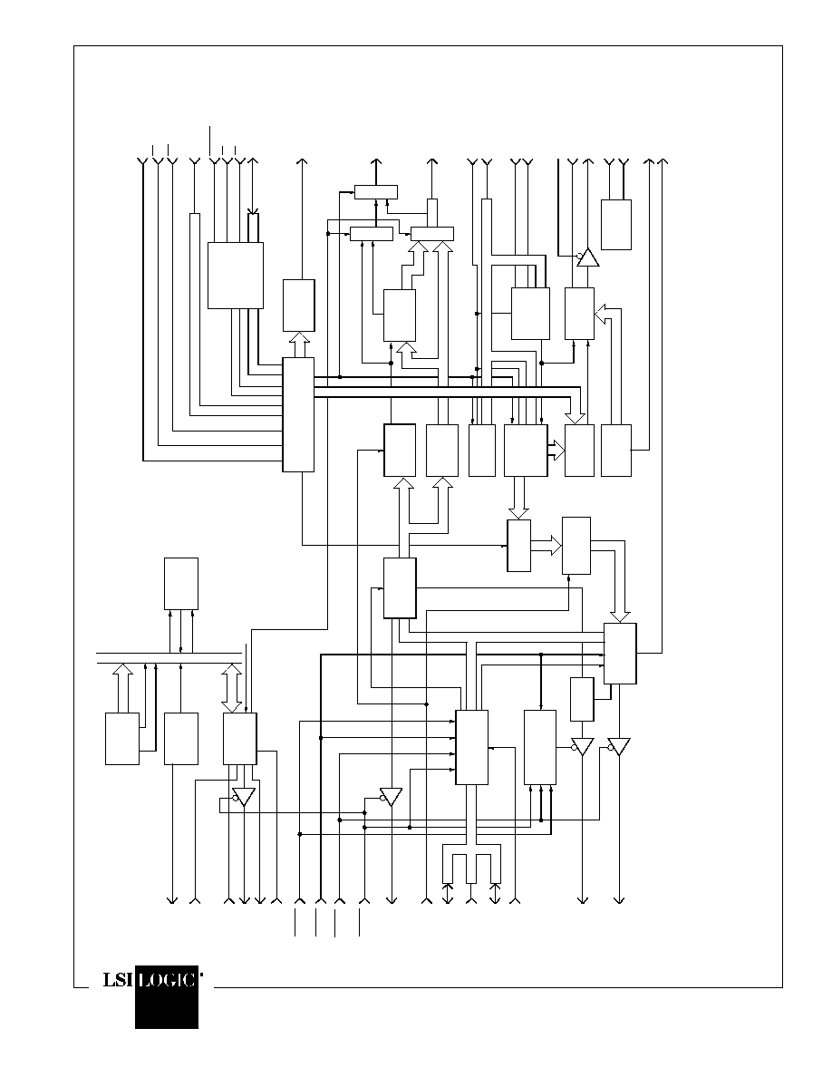
Figure 1. 80C300 Functional Block Diagram
T16COLL
BUSMODE
RXOVF
RXBYT12
BUSSIZE
BE1
BE0
ENREGIO
Figure 1. 80C200 Functional Block Diagram

80C200
4-4
4
MD400179/≠
CDST5
CDST6
CDST7
CDST4
VDD
A3
A2
A4
VDD
GND
CDST8
CDST9
CDST10
A5
CDST11
CDST12
CDST13
GND
CDST14
CDST15
CLRTXERR
CLRRXERR
TXWREN
TXINTEN
RXINTEN
RXTXBE0
RXTXBE1
VDD
VDD
TXRET
INT
RXABORT
RXDC
RXRDY
TXRDY
TXNOCRC
RXTXEOF
SPDTAVL
RESET
RXRDEN
SYS_CLK
RXTXDATA10
RXTXDATA11
RXTXDATA9
RXTXDATA8
VDD
RXTXDATA6
RXTXDATA5
RXTXDATA4
RXTXDATA3
RXTXDATA2
GND
RXTXDATA7
GND
VDD
RXTXDATA16
RXTXDATA15
RXTXDATA14
RXTXDATA13
RXTXDATA12
RXTXDATA21
RXTXDATA20
RXTXDATA19
RXTXDATA18
RXTXDATA17
GND
RXC
GND
GND
RXTXDATA1
RXTXDATA0
GND
FDUPLX
MDC
TXD2
TXD1
TXD0
TXEN
COLL
MDIO
TXD3
TXC
RXD3
RXD0
CSN
RX_DV
RD
WR
BE1
BE0
T16COLL
RXOVF
RXBYT12
RX_ER
1
6
5
4
3
2
7
12
11
10
9
8
13
18
17
16
15
14
19
24
23
22
21
20
28
27
26
25
29
34
33
32
31
30
38
37
36
35
A1
A0
CDST1
CDST2
CDST3
CDST0
BUSMODE
BUSSIZE
ENREGI0
RXTXBE3
GND
VDD
RXTXBE2
GND
39
45
44
43
42
41
40
46
52
51
50
49
48
47
55
54
53
56
62
61
60
59
58
57
64
63
VDD
GND
65
71
70
69
68
67
66
72
78
77
76
75
74
73
81
80
79
82
88
87
86
85
84
83
91
90
89
92
98
97
96
95
94
93
101
100
99
102
RXTXDATA22
GND
RXTXDATA26
RXTXDATA25
RXTXDATA24
RXTXDATA23
RXTXDATA27
RXTXDATA28
GND
GND
RXTXDATA31
RXTXDATA30
RXTXDATA29
103
107
106
105
104
108
112
111
110
109
113
117
116
115
114
118
122
121
120
119
123
127
126
125
124
DAISY_OUT
128
RXD2
RXD1
GND
GND
Figure 2. 80C200 Pin Configuration
80C200
128 PQFP
80C200
4-5
5
MD400179/≠
1.0 PIN DESCRIPTION
Pin
Pin Name
I/O
Description
Chip Register Interface
32
ENREGIO
I
This active low input enables the chip for register operations. This input must be low
before any registers can be written or read.
3
WR
I
Within the chip, this input acts as a write strobe for one of the registers and the register
is addressed through the A[5:0] address inputs. The data being written appears on the
CDST[15:0] data lines and must be set up relative to the rising edge of the write strobe.
This input is active low.
4
RD
I
This input acts as a read strobe for one of the registers and the register is addressed
through the A[5:0] address inputs. When the read strobe is active low, the output
drivers for CDST[15:0] data bus are enabled. Valid register data appears on the data
bus a specified time before the rising edge of the read strobe.
7-12
A[5:0]
I
These inputs are the address lines used to select which register is being read or written.
33
BUSSIZE
I
This input when HIGH sets the register interface of the 80C200 to 16-bit mode and
when LOW to 8-bit mode. In 8-bit mode only CDST[7:0] of the CDST data bus is used
for register accesses.
6, 5
BE[1:0]
I
These inputs are active LOW byte enables to enable byte wide register accesses when
the 80C200's register interface is in 16-bit mode.
13-17
CDST[15:0]
I/O
These bidirectional lines carry register data to or from the internal registers of the chip.
20-25
These lines are nominally high impedance until their output drivers are enabled by the
27-31
RD and ENREGIO input pins being driven low.
59
INT
O
This output is driven high by a variety of transmit and receive interrupt conditions.
It remains high until the status register containing the reason for the interrupt is read.
62
RESET
I
This input is an active low asynchronous chip reset. After reset, all registers except
the Hash and Station Address registers are reset to zero, all FIFOs are cleared, all
counters are reset to zero.
Receive and Transmit FIFO Interface
34
BUSMODE
I
This input when HIGH sets the FIFO interface to Big Endian mode. In this mode data
written to the transmit FIFO is transmitted most significant byte first. When this pin is
LOW, Little Endian transmit order is used.
43
RXINTEN
I
This is an active low input that acts as a chip enable to enable the receiver interface.
Driving this pin active, enables the output drivers for the RXDC, RXRDY pins. Also, this
pin must be driven active before receive FIFO reads can be performed.
44
TXINTEN
I
This is an active low input that acts as a chip enable to enable the transmitter interface.
Driving this pin active enables the output drivers for the TXRET, TXRDY pins. Also, this
pin must be driven active before transmit FIFO writes can be performed.
46
RXRDEN
I
This is an active low input that, when driven active with the RXINTEN pin, enables read
operations from the receive FIFO within the chip.
47
TXWREN
I
This is an active low input that, when driven active with the TXINTEN pin, enables write
operations to the transmit FIFO within the chip.
45
SYS_CLK
I
This is the system clock acting as the chip's read/write strobe to receive/transmit
FIFO. With the TXINTEN and TXWREN inputs active low, this input becomes the
write strobe for writing transmit data to the chip's transmit FIFO. Similarly, with the
RXINTEN and RXRDEN inputs active low, this input becomes the read strobe for
reading receive data from one of the chip's receive FIFO. This input must be connected
to a continuous clock whose maximum frequency can be 33 MHz.