 | –≠–ª–µ–∫—Ç—Ä–æ–Ω–Ω—ã–π –∫–æ–º–ø–æ–Ω–µ–Ω—Ç: 84C24 | –°–∫–∞—á–∞—Ç—å:  PDF PDF  ZIP ZIP |
84C24
4-1
MD400147/A
1
96200
84C24
Quad 10Base-T Ethernet
Media Interface Adapter
- Transmit Disable
- Programmable LED Output
- Loopback
s
Status Outputs
- Link
- Polarity
- Jabber
- Full Duplex
- AutoNegotiation
- Interrupt
s
LED Outputs
- Link
- Full Duplex
- User Programmable
s
Serial Port For Configuration And Status
s
68L PLCC
Features
s
Single Chip Interface Between Ethernet Controller
And Twisted Pair Wire
s
Four Independent Channels In One IC
s
On Chip Wave Shaping And Filters - No External
Filters Required
s
Few External Components
s
Meets All Applicable IEEE 802.3 and 10Base-T
Standards
s
Direct Interface To SEEQ, Intel, AMD, NSC
Controllers
s
Full/Half Duplex AutoNegotiation Per
IEEE 802.3 Clause 28
s
Many User Features And Options
- Half/Full Duplex AutoNegotiation
- Universal Controller Interface
- Autopolarity
- Smart Squelch
- Transmit Level Adjust
- Receive Level Adjust
- 100/150 Ohm Cable
- Powerdown
- SQE Disable
- Link Disable
- Jabber Disable
84C24
44
PLED2
PLED1
PLED3
CS
INT
GND3
GND5
SDIO
SCLK
OSCIN
10
10
26
10
21
20
19
18
17
16
15
14
13
12
11
24
22
23
PLED0
RESET
GND2
VCC2
VCC3
9
8
2
1 68 67
3
4
5
6
7
27
RXC0
TXEN1
TXD1
RXD1
CSN1
RXC1
COL0
TXEN0
TXD0
RXD0
CSN0
V
CC5
Pin Configuration
84C24
68 Pin PLCC
Top View
Full Duplex
Note: Check for latest Data Sheet revision
before starting any designs.
SEEQ Data Sheets are now on the Web, at
www.lsilogic.com.
This document is an LSI Logic document. Any
reference to SEEQ Technology should be
considered LSI Logic.

84C24
4-2
MD400147/A
2
84C24 Table of Contents
1.0 Pin Description
2.0 Block Diagram
3.0 Functional Description
3.1 Introduction
3.2 General
3.3 Controller Interface
3.4 Manchester Encoder
3.5 Manchester Decoder
3.6 Twisted Pair Transmitter
3.6.1 Transmitter
3.6.2 Transmit Level Adjust
3.6.3 Transmit Disable
3.6.4 STP Cable Mode
3.7 Twisted Pair Receiver
3.7.1 Receiver
3.7.2 Squelch
3.7.3 Receive Level Adjust
3.8 Start of Idle (SOI)
3.9 Link Integrity and AutoNegotiation
3.9.1 General
3.9.2 10Base-T Link Algorithm
3.9.3 AutoNegotiation Algorithm
3.9.4 Link Indication
3.9.5 Link Disable
3.10 Collision
3.11 Signal Quality Error (SQE)
3.12 Jabber
3.13 Receive Polarity Correction
3.14 Full Duplex
3.15 Loopback
3.16 Reset
3.17 Powerdown
3.18 Oscillator
3.19 LED Drivers
3.20 Serial Port
3.20.1 Signal Description
3.20.2 Timing and Multiple Register Access
3.20.3 Frame Structure
3.20.4 Bit Types
3.20.5 Interrupt
3.20.6 Register Structure
4.0 Register Description
5.0 Application Information
5.1 Example Schematics
5.2 TP Transmit Interface
5.3 TP Receive Interface
5.4 TP Transmit Output Current Set
5.5 Controller Interface
5.6 Serial Port
5.6.1 General
5.6.2 Polling vs. Interrupt
5.6.3 Serial Port Addressing
5.7 Reset
5.8 Diagnostic Loopback
5.9 Oscillator
5.10 LED Drivers
5.11 Power Supply Decoder
6.0 Specifications

84C24
4-3
MD400147/A
3
1.0 Pin Description
Pin
Pin Name
I/O
Description
45
V
CC
8
--
Positive Supply. 5V
±
5%.
47
V
CC
7
59
V
CC
6
3
V
CC
5
55
V
CC
4
18
V
CC
3
23
V
CC
2
25
V
CC
1
44
GND 8
--
Ground. 0 Volts.
46
GND 7
60
GND 6
12
GND 5
64
GND 4
21
GND 3
24
GND 2
26
GND 1
42
TPO 3+
O
Twisted Pair Transmit Output, Positive.
38
TPO 2+
33
TPO 1+
29
TPO 0+
43
TPO 3≠
O
Twisted Pair Transmit Output, Negative.
39
TPO 2≠
34
TPO 1≠
30
TPO 0≠
40
TPI 3+
I
Twisted Pair Transmit Input, Positive.
36
TPI 2+
31
TPI 1+
27
TPI 0+
41
TPI 3 ≠
I
Twisted Pair Transmit Input, Negative.
37
TPI 2 ≠
32
TPI 1 ≠
28
TPI 0 ≠
35
REXT
O
Transmit Current Set. An external resistor connected between this pin
and GND will set the output current supplied on TPO[3:0]
±
.
51
TXC
O
Transmit Clock Output. This controller interface output provides a 10 Mhz
clock to the controller. Transmit data from the controller on TXD is clocked in
on edges of TXC and OSCIN.
49
TXEN 3
I
Transmit Enable Input. This controller interface input has to be asserted
57
TXEN 2
when data on TXD is valid.
66
TXEN 1
5
TXEN 0
50
TXD 3
I
Transmit Data Input. This controller interface input contains data to be
58
TXD 2
transmitted on the TP transmit output and is clocked in on edges of TXC
67
TXD 1
and OSCIN.
6
TXD 0

84C24
4-4
MD400147/A
4
Pin
Pin Name
I/O
Description
54
RXC 3
O
Receive Clock Output. This controller interface output provides a 10 Mhz
63
RXC 2
clock to the controller. Receive data on RXD is clocked out to the
2
RXC 1
controller on edges of RXC.
9
RXC 0
53
CSN 3
O
Carrier Sense Output. This controller interface output is asserted when
62
CSN 2
valid data is present on the RXD output.
1
CSN 1
8
CSN 0
52
RXD 3
O
Receive Data Output. This controller interface output contains receive
61
RXD 2
data from the TP input and is clocked out on edges of RXC.
68
RXD 1
7
RXD 0
48
COL 3
O
Collision Output. This controller interface output is asserted when
56
COL 2
collision between transmit and receive data occurs.
65
COL 1
4
COL 0
22
OSCIN
I
Clock Oscillator Input. There must be either a 10 Mhz crystal or a 10
Mhz clock tied between this pin and GND. TXC output is generated from
this input.
15
PLED 3 (SA3)
I/O
Programmable LED Outputs/Serial Port Address Inputs. These pins
16
PLED 2 (SA2)
Open
are normally outputs and can be programmed through the serial port to be
17
PLED 1 (SA1)
Drain
either a Link Pulse Detect Ouput, Full Duplex Detect Output, or user select
19
PLED 0 (SA0)
Pullup
output. These pins can drive an LED from V
CC
.
During powerup or reset, these are inputs and the value on these pins is
latched in and used as the serial port device address.
13
CS
I
Serial Port Chip Select Input. This pin enables the serial port for I/O
operation.
10
SCLK
I
Serial Port Clock Input. This clock shifts serial port data into SDIO on
falling edges and out of SDIO on falling edges.
11
SDIO
I/O
Serial Port I/O Data. This bidirectional pin contains serial port data that
is clocked in and out on falling edges of SCLK.
14
INT
O
Serial Port Interrupt Output. This output is asserted whenever there is
Open
a change in certain serial port read bits, and deasserted after these bits are
Drain
read. This pin consists of an open drain output transistor with a resistor
Pullup
pullup.
20
RESET
I
Reset Input.
Pullup
1 = Normal
0 = Device In Reset State
Pin Description (continued)
84C24
4-5
MD400147/A
5
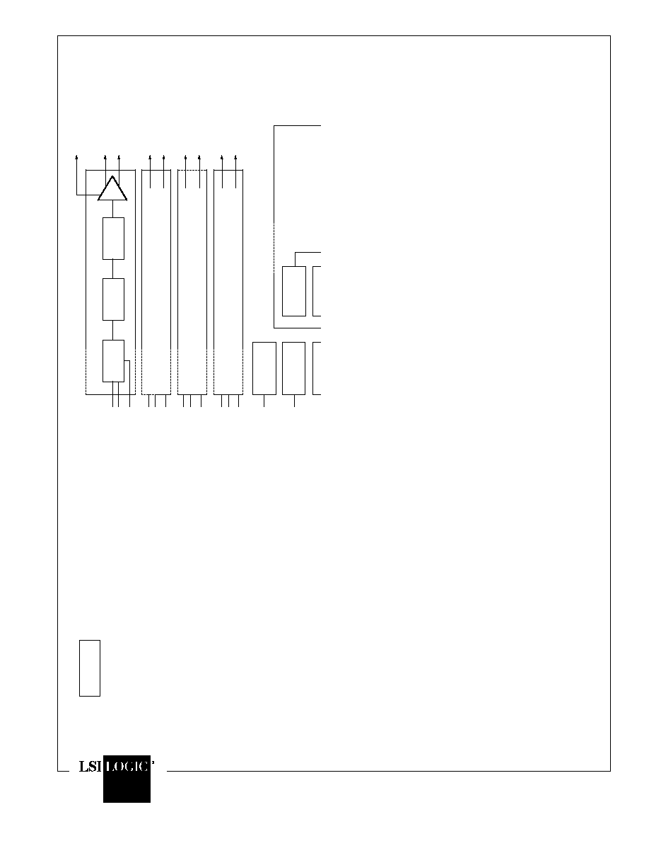
2.0 Block Diagram
LP
FILTER
DAC
+
≠
RECEIVER
ROM
TRANSMITTER
TPO0+
TPO2≠
TPO2+
TPO1≠
TPO1+
TPO0≠
TPO3≠
TPO3+
REXT
CLOCK GEN
LINK PULSE
GEN
SOI
GEN
AUTONEG.
POLARITY