Flip Chip Ball Grid Array (FPBGA) Package Family
Overview
LSI Logic's FPBGA packages offer flip chip die interconnect, and support
leadcounts in excess of 1700 to target high performance, high pin count appli-
cations. LSI Logic is the first company to qualify a flip chip package using
organic laminate substrates. Organic laminate substrates have better perfor-
mance through copper interconnect and also have a lower dielectic constant.
The FPBGA is lower in cost than conventional ceramic or the latest glass
ceramic materials.
Description
Flip chip packages differ from the traditional wire bonded packages in that the
silicon chip does not have a ring of wire bond pads around its perimeter.
Instead, the chip is covered across its top surface by a matrix of solder bumps.
The chip is then "flipped" over and attached to the package substrate using
solder reflow techniques.
FPBGA provides the highest electrical performance available today through
the elimination of the wire bond, separate core and I/O power and ground,
reference planes, and the lowest available dielectric constant.
In addition, this innovative package family has excellent thermal perfor-
mance. The backside of the flipped die is attached directly to a heatspreader
which covers the entire package. If necessary, a heatsink can be added. The
organic laminate substrate has a Thermal Coefficient of Expansion (TCE)
which is a much closer match to PCB material than glass ceramic substrates.
This enables package body sizes of up to 45mm per side to be available to the
designer. Conventional ceramic BGA packages are limited to 35mm per side.
LSI Logic is offering a choice of two different organic substrate materials,
namely BT laminate and MicrolamTM buildup. The Microlam buildup offers
the benefit of finer bump and interconnect feature sizes.
Designed for maximum electrical
performance
Features
∑
Stripline I/O traces between power and
ground planes
∑
Low inductance power and ground planes
∑
Core voltage and ground isolated and routed
directly to solder balls under die
∑
Segmented power planes
∑
100% differential or single-ended I/Os
∑
Ratio of signals:power:ground is 4:1:1
∑
Low dielectric constant in organic laminate
materials
Benefits
∑
Controlled impedance I/O traces
∑
High integrity core power supplies with
thermal path to PCB
∑
Multiple low inductance I/O voltages
∑
Suited for high-speed differential signals up to
2.4 Gbit/s
∑
Low power supply noise
∑
Reduced cross-talk
∑
Improved signal propagation delay
Designed for maximum thermal
performance
Features
∑
Copper heatspreader covers entire package
∑
Direct thermal contact to flip chip die
Benefits
∑
Heatsink can be attached for increased perfor-
mance
∑
Low thermal impedance path from chip to
ambient surroundings
Ball Count
Body Size
#I/O
Array
Vss
Vdd
VssC
VddC
788
31
504
30 x 30
124
124
18
18
960
35
600
34 x 34
148
148
32
32
1157
40
720
39 x 39
176
180
41
40
1413
40
864
39 x 39
212
216
61
60
1728
45
1024
44 x 44
252
256
98
98
Flip Chip Ball Grid Array (FPBGA) Package Family
LSI Logic and LSI Logic logo design are registered trademark
of LSI Logic Corporation. All other brand and product
names may be trademarks of their respective companies.
LSI Logic Corporation reserves the right to make changes to
any products and services herein at any time without notice.
LSI Logic does not assume any responsibility or liability aris-
ing out of the application or use of any product or service
described herein, except as expressly agreed to in writing by
LSI Logic; nor does the purchase, lease, or use of a product
or service from LSI Logic convey a license under any patent
rights, copyrights, trademark rights, or any other of the intel-
lectual property rights of LSI Logic or of third parties.
Copyright ©1999 by LSI Logic Corporation.
All rights reserved.
For more information please call:
Europe +32.11.300.351
408.433.7700 Dept. JDS
www.lsilogic.com
LSI Logic Corporation
North American Headquarters
Milpitas, CA
Tel: 408.433.8000
LSI Logic Europe Ltd
European Headquarters
United Kingdom
Tel: 44.1344.426544
Fax: 44.1344.481039
LSI Logic KK Headquarters
Tokyo, Japan
Tel: 81.3.5463.7821
Fax: 81.3.5463.7820
Order No. B20022
599.1K.CM.L ≠ Printed in USA
ISO 9000 Certified
Complete Packaging Portfolio
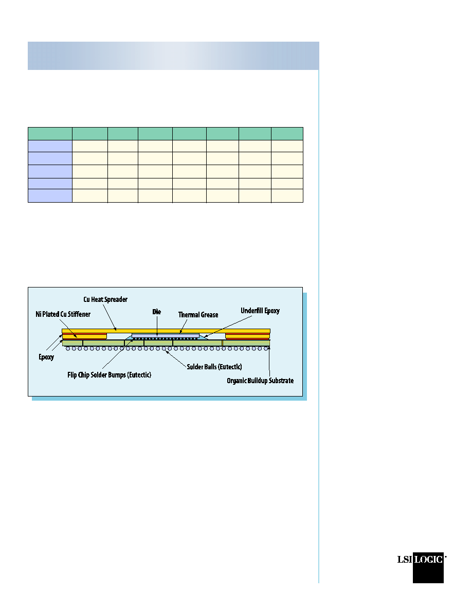
The design and construction of LSI's multilayer laminate flip chip package
provides superior electrical and thermal characteristics for a wide range of
performance leading and high lead count applications in computing, network-
ing and telecommunications.
FPBGA Package Family
Laminate Flip Chip Materials & Construction
LSI Logic's packaging portfolio offers a wide range of application focused pack-
ages ranging from low-cost packages for mainstream applications to Ball Grid
Arrays optimized for the most demanding applications. These products are
designed to meet a wide variety of thermal and electrical performance require-
ments with a focus on die size optimization, high I/O utilization, surface mount
capability, and high reliability.