 | –≠–ª–µ–∫—Ç—Ä–æ–Ω–Ω—ã–π –∫–æ–º–ø–æ–Ω–µ–Ω—Ç: G12-p3.3V | –°–∫–∞—á–∞—Ç—å:  PDF PDF  ZIP ZIP |
February 2001
1
Copyright © 2000, 2001 by LSI Logic Corporation. All rights reserved.
G12TM-p 3.3 V, 4 mA,
5-Volt Tolerant, Fail-Safe,
General Purpose I/O Buffers
Datasheet
LSI Logic Corporation provides the following driver/receiver input/output
(I/O) cells for use as general purpose I/O buffers:
The I/O buffers provide off-chip, bidirectional I/O signaling for application-
specific integrated circuit (ASIC) chips implemented in the LSI Logic
G12TM-p 0.13
µ
m process technology. Functionally similar, the I/O buffers
(
Figure 1
) provide an ASIC application with different driver options.
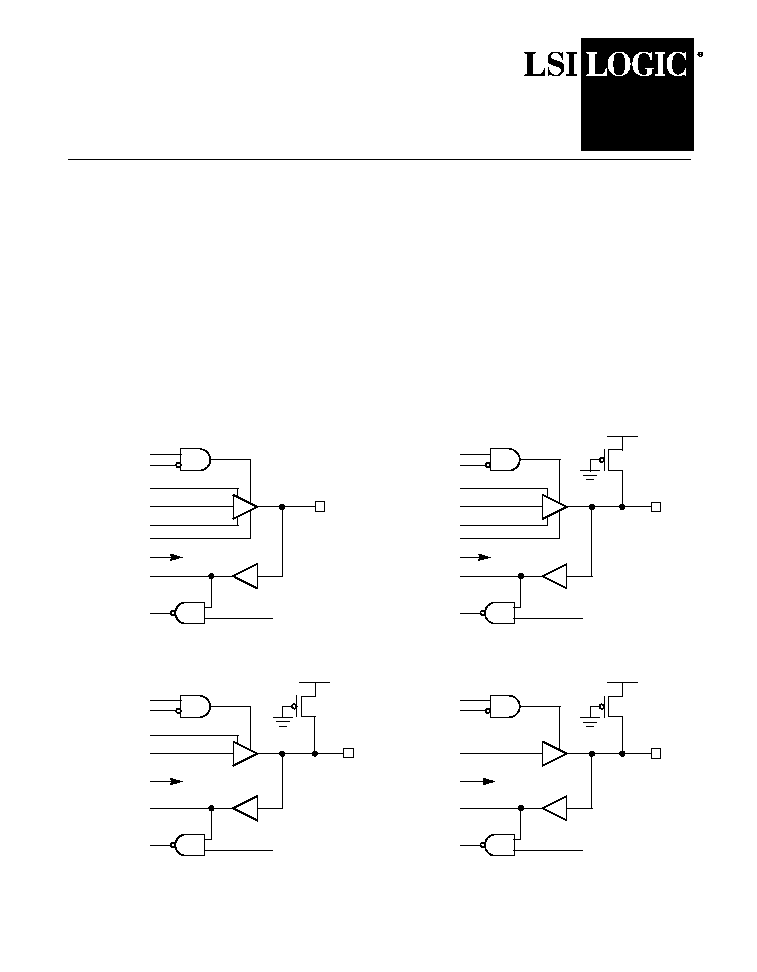
Figure 1
Buffer Block Diagrams
∑
bd4f5fsls33
∑
bd4puf5fsls33
∑
bd4puodf5fsls33
∑
bd4puodf5fscls33
PI
TN
EN
A
Z
PO
IO
IDDTN
T
D
CEN
PI
TN
EN
A
Z
PO
IDDTN
CEN
PI
TN
EN
A
Z
PO
IO
IDDTN
T
D
CEN
PI
TN
EN
A
Z
PO
IO
IDDTN
I/O Pad
I/O Pad
I/O Pad
IO
I/O Pad
a) bd4f5fsls33
b) bd4puf5fsls33
c) bd4puodf5fsls33
d) bd4puodf5fscls33

2
G12TM-p 3.3 V, 4 mA, 5-Volt Tolerant, Fail-Safe, General Purpose I/O Buffers
Features and Benefits
Signal Descriptions
Table 1
describes signal connections for all four buffers.
∑
Up to 20 MHz,
3.3 V I/O operation
∑
5-Volt tolerant
∑
Fail-safe at high voltages
∑
Feedthrough protection
∑
20
µ
A maximum leakage current
∑
Minimum 4 mA current drive
into a 40 pF load at 20 MHz
∑
1.8 V internal signaling for
reduced power consumption
∑
Uses one standard I/O slot
Table 1
I/O Buffer Connections
Signal
Direction
Description
A
IN
Data input to I/O buffer driver from ASIC circuitry
CEN
1
1. Not available in bd4puodf5fscls33
IN
Enables I/O buffer operation after power-on
D
2
2. Available only in bd4f5fsls33 and bd4puf5fsls33. Refer to
Table 4
for settings.
IN
Configures driver operating mode
EN
IN
0 = Normal mode
1 = Disable I/O buffer driver
IDDTN
IN
0 = Power down entire cell
3
1 = Normal mode
3. Used for production IDDQ leakage test
PI
IN
NAND-tree parametric test input
T
2
IN
Configures driver operating mode
TN
IN
0 = Disable I/O buffer driver
1 = Normal mode
IO
IN/OUT
Input/output pad
PO
OUT
NAND-tree parametric test output
Z
OUT
I/O buffer receiver output to ASIC circuitry

G12TM-p 3.3 V, 4 mA, 5-Volt Tolerant, Fail-Safe, General Purpose I/O Buffers
3
General Description
The buffers include a receiver, driver, and NAND-tree circuitry to conform
with standard LSI Logic test methodology. The buffers translate signals
between the 1.8 V operating levels of the ASIC core circuitry and the
3.3 V operating levels at the I/O pad. They tolerate high DC and transient
voltages at the I/O pad, are fail safe, and provide feedthrough protection.
Voltage Tolerance
The I/O buffers are 5-volt tolerant. Although the off-chip I/O signaling
normally operates at 3.3 volts, external circuitry may cause higher
voltages, typically upwards of 5 volts, to appear at the chip I/O pad.
Circuit and process techniques ensure that such DC or transient voltages
do not damage the I/O buffer circuitry.
Failure and Feedthrough Protection
In the absence of a V
DD
supply, the I/O buffers are fail-safe and protected
against voltage feedthrough. With high voltage applied to the chip I/O
pad, the I/O buffers can survive without degradation for up to ten years.
Furthermore, with a low, maximum 20
µ
A leakage current, the high
voltage can not power up the ASIC through voltage feedthrough.
Functional Description of Receivers
The buffers use the same receiver circuitry. The following truth table
(
Table 2
) describes receiver behavior.
Table 2
Receiver Truth Table
Inputs
Outputs
IDDTN
IO
PI
Z
PO
0
1
1. Factory IDDQ test setting
High Impedance
1
1
0
1
0
0
0
1
1
1
0
1
1
1
1
1
1
0

4
G12TM-p 3.3 V, 4 mA, 5-Volt Tolerant, Fail-Safe, General Purpose I/O Buffers
Functional Description of Drivers
The buffers use similar driver circuitry that produces a minimum of 4 mA
of output drive. The buffers provide options for selecting the driver output
configuration and power-up mode (
Table 3
). All the buffers except
bd4f5fsls33
have internal pull-up resistor devices. Preset power-up
modes avoid unpredictable output behavior.
Driver Output Configuration
With the
bd4f5fsls33
(
Figure 1
a) or
bd4puf5fsls33
(
Figure 1
b) buffer,
the T and D inputs set a driver output to open-drain, open-source, or
totem-pole mode (
Table 4
). An application can hardwire the T and D
inputs, or, to dynamically configure a driver output, it can supply the T
and D inputs from a register.
Table 3
I/O Buffer Driver Characteristics
I/O Buffer Cell
Driver Mode
Pull-Up
Power-Up Mode
Application
bd4f5fsls33
Dynamically programmable open-drain,
open-source, or totem-pole output
None
3-State
General
bd4puf5fsls33
Dynamically programmable open-drain,
open-source, or totem-pole output
Yes,
internal
3-State
General
bd4puodf5fsls33
Open-drain output
Yes,
internal
Current sinking
logic level 0
Power-on
reset
bd4puodf5fscls33
Open-drain output
Yes,
internal
3-State
General
Table 4
Driver Output Mode Selection
T
D
Output
0
0
Open drain
0
1
Totem pole
1
0
Totem pole
1
1
Open source

G12TM-p 3.3 V, 4 mA, 5-Volt Tolerant, Fail-Safe, General Purpose I/O Buffers
5
The
bd4puodf5fsls33
(
Figure 1
c) and the
bd4puodf5fscls33
(
Figure 1
d) buffers fix the output in the open-drain mode.
Pull-Up Resistor
Except for
bd4f5fsls33
, the buffers include a pull-up resistor, which can
provide from 100
µ
A to 500
µ
A of current across the specified process,
voltage, and temperature ranges.
Note:
Evaluate the buffer models before simulating a design.
Models provided for some third-party design environments
may not correctly represent or even include the pull-up
resistor.
Power-Up Modes
Each buffer has a defined power-up mode (
Table 3
) to avoid
unpredictable output behavior. The
bd4f5fsls33
,
bd4puf5fsls33
, and
bd4puodf5fsls33
buffers preset the driver output to 3-state or current-
sinking mode upon power up. The
bd4puodf5fscls33
buffer has no
preset power-up mode.
Preset to 3-State (bd4f5fsls33 and bd4puf5fsls33)
At power up, circuitry in the
bd4f5fsls33
and
bd4puf5fsls33
buffers
forces the IO signal at the I/O pad to the high-impedance state. To begin
normal operation, the buffers require the ASIC application to assert CEN
to HIGH.
Preset to Open-Drain (bd4puodf5fsls33)
At power up, circuitry in the
bd4puodf5fsls33
buffer forces the driver
output to open-drain mode. As the driver sinks current, it drives the IO
signal at the I/O pad to LOW. Designed primarily for power-on-reset
applications, the buffer holds circuits connected to the I/O pad in the
LOW reset state until the ASIC application asserts CEN to HIGH, thereby
releasing the buffer to operate normally.
To drive the CEN signal HIGH directly from a source external to the
ASIC, connect CEN to a DDRV type I/O pad for ESD protection and
apply an activation signal. Although this activation signal may reach
3.3 V, a signal limited to1.8 V better matches the normal internal
signaling level, and is therefore preferable.