
May 2001
1
Copyright © 2001 by LSI Logic Corporation. All rights reserved.
G12TM-p ATA100 3.3 V,
5-Volt Tolerant, Fail-Safe
I/O Buffer
Datasheet
The ATA100 I/O buffer provides on-chip input/output (I/O) signaling for
application-specific integrated circuit (ASIC) chips implemented in the
LSI Logic G12TM-p 0.13
µ
m process technology. The buffer operates at
data transfer rates of up to 100 Mbytes/s in ATA
1
applications. An ATA100
bus system of I/O buffers consists of the following cell types:
An ATA100 bus system with one
atabiasls33
bias cell may include up
to forty
ata100f5fsls33
bidirectional buffer cells.
Features and Benefits
1. Advanced Technology Attachment protocol established by Technical Committee 13 (T13) of
the National Committee on Information Technology Standards (NCITS) under the auspices
of the American National Standards Institute (ANSI).
Cell Type
Name
Function
Buffer
ata100f5fsls33
Bidirectional signaling
Bias
atabiasls33
Sets operating level of buffer cells
Support
atacornerls33
ATA100 corner cell
atapvddio33
3.3 V I/O power pad cell
atapvssio33
3.3 V I/O ground pad cell
atapvdd33
1.8 V core power pad cell
atapvss33
1.8 V core ground pad cell
atadvddls33
3.3 V ESD protection cell
atadvdd2ls33
1.8 V ESD protection cell
∑
3.3 V I/O operation
∑
100 Mbytes/s data transfer
∑
5-Volt tolerant
∑
Fail-safe at high voltages
∑
Feedthrough protection
∑
20
µ
A maximum leakage current
∑
Programmable driver slew rate
∑
Minimum 4 mA current drive
into a 25 pF load at 26.3 MHz
∑
1.8 V internal signaling for
reduced power consumption
∑
Uses two standard I/O slots

2
G12-p ATA100 3.3 V, 5-Volt Tolerant, Fail-Safe I/O Buffer
General Description
One application of the ATA100 buffer is for storage devices such as hard
disk and optical drives that attach to the popular IDE
1
bus. In a 16-bit
wide IDE bus application transferring data on both clock edges, for
example, the ATA100 bus system transfers data at 100 Mbytes/s with a
25 MHz clock. Maximum clock frequency for the buffer is 26.3 MHz.
The ATA100 buffer includes level translation circuitry. It receives 1.8 V
level signals from the ASIC circuitry and produces 3.3 V level output at
the I/O pad. Similarly, it receives off-chip input at 3.3 volts and translates
it to 1.8 volts for the internal ASIC application. Power saving features
minimize power consumption.
The ATA100 buffer is 5-volt tolerant and fail-safe and protects against
voltage feedthrough as follows:
∑
Voltage Tolerance
Although the off-chip I/O signaling normally operates at 3.3 V,
external circuitry may cause higher voltages, typically 5 volts, to
appear at the chip I/O pad. Circuit and process techniques ensure
that such DC or transient voltages do not damage the buffer circuitry.
∑
Safe from Failure
The buffer will not fail if a high voltage persists at the I/O pad even
with the V
DD
supply removed. Under such conditions the buffer can
survive without degradation for up to ten years.
∑
Feedthrough Protection
In the absence of a V
DD
supply and with high voltage applied at the
I/O pad, the low, maximum 20
µ
A leakage current of the buffer
prevents voltage feedthrough from powering up the ASIC.
The ata100f5fsls33 Buffer Cell
The
ata100f5fsls33
buffer cell (
Figure 1
) contains a receiver, a 3-state
driver with programmable slew rate, and test circuitry. The driver slew
1. Integrated Drive Electronics
G12-p ATA100 3.3 V, 5-Volt Tolerant, Fail-Safe I/O Buffer
3
rate depends on the bias current from the bias cell. Refer to
"The
atabiasls33 Bias Cell"
section for programming the slew rate.
Figure 1
ata100f5fsls33 Block Diagram
Built-in NAND-tree logic gates and IDDTN control for IDDQ leakage
testing enable use of the standard LSI Logic test methodology.
Signal Descriptions
Table 1
describes the
ata100f5fsls33
connections.
PI
TN
EN
A
Z
PO
IO
IDDTN
Chip I/O Pad
Receiver
Driver
IBIAS
Table 1
ata100f5fsls33 Connections
Signal
Direction
Description
A
IN
Data input to driver from ASIC circuitry
EN
IN
Enable 3-state output mode:
0 = Normal mode
1 = Disable driver with output in high-impedance mode
IBIAS
IN
Bias current input from bias cell
IDDTN
IN
0 = Power down entire cell
1
1 = Normal mode
1. Used for production IDDQ leakage test
PI
IN
NAND-tree parametric test input
TN
IN
Alternate or test connection to enable 3-state output mode:
0 = Disable driver with output in high-impedance mode
1 = Normal mode
IO
IN/OUT
Input/output pad
PO
OUT
NAND-tree parametric test output
Z
OUT
Receiver buffer output to ASIC circuitry

4
G12-p ATA100 3.3 V, 5-Volt Tolerant, Fail-Safe I/O Buffer
Receiver Truth Table
Table 2
describes the
ata100f5fsls33
receiver behavior.
Driver Truth Table
Table 3
describes the
ata100f5fsls33
driver behavior.
Storage Application Example
The DASP
1
line in a disk controller requires a driver with an open-drain
output. To configure the driver (
Figure 2
) in the
ata100f5fsls33
cell,
connect the A input to ground. This disables the VDD side of the output
and produces an open-drain output (
Figure 3
).
Table 2
Receiver Truth Table
Inputs
Outputs
IDDTN
IO
PI
Z
PO
0
1
1. Factory IDDQ test setting
High Impedance 1
1
0
1
0
X
2
2. Don't care state, X = 0 or 1
0
1
1
1
0
1
1
1
1
1
1
0
Table 3
Driver Truth Table
IDDTN
A
TN
EN
IO
0
1
1. Factory IDDQ test setting
X
2
2. Don't care state, X = 0 or 1
X
X
High Impedance
1
X
X
1
High Impedance
1
X
0
X
High Impedance
1
0
1
0
0
1
1
1
0
1
1. Device active or slave present

G12-p ATA100 3.3 V, 5-Volt Tolerant, Fail-Safe I/O Buffer
5
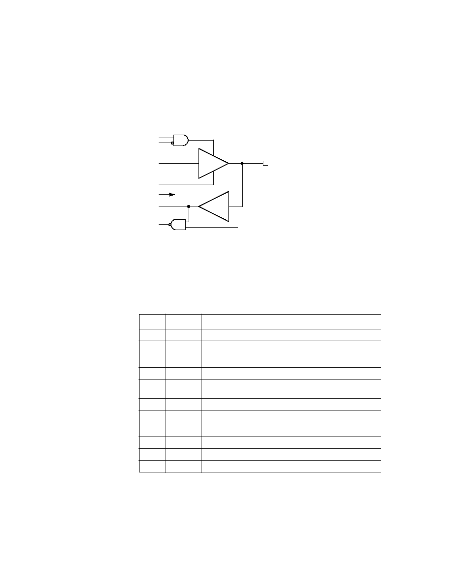
Figure 2
Driver with 3-State Output Enable Circuit
Figure 3
Driver Configured for Open-Drain Output
For data input to the configured driver, use EN or TN. For example, send
positive-logic data to EN and set TN = 1, the normal mode. Applying
data, EN = 1 forces IO to the high-impedance state. With EN = 0, the IO
output sinks current, which pulls the output LOW.
Alternatively, send negative-logic data to TN and set EN = 0, the normal
mode. Applying data, TN = 0 forces IO to the high-impedance state. With
TN = 1, the IO output sinks current, which pulls the output LOW.
Specifications
The buffer adheres to the general specifications in
Table 4
.
Table 5
describes the driver DC characteristics.
Table 6
describes the receiver
DC characteristics.
TN
EN
A
IO
VDD
IO
EN
TN
Table 4
General Specifications
Symbol
Parameter
Condition
Min.
Typ. Max.
Unit
V
DD
Supply voltage
2.97
3.3
3.63
V
T
j
Junction temperature
0
≠
125
∞C
ESD
Electrostatic discharge,
human body model (HBM)
MIL-STD-883C,
Method 3015.7
100 pF @1.5 K
2000
≠
≠
V
Electrostatic discharge,
charged device model (CDM)
ESD DS5.3.1-1996
500
≠
≠
V