 | –≠–ª–µ–∫—Ç—Ä–æ–Ω–Ω—ã–π –∫–æ–º–ø–æ–Ω–µ–Ω—Ç: L64733 | –°–∫–∞—á–∞—Ç—å:  PDF PDF  ZIP ZIP |
August 2000
1
Copyright © 1999, 2000 by LSI Logic Corporation. All rights reserved.
L64733/L64734
Tuner and Satellite
Receiver Chipset
Datasheet
The L64733/34 chipset is designed specifically to meet the needs of
satellite broadcast digital TV and is compliant with the European digital
video broadcast (DVB-S) standard and the technical specifications for
DSS systems. The chipset forms a complete "L-Band to bits" system.
A typical application of the L64733/34 chipset is satellite digital TV
reception in accordance with ETS 300 421.
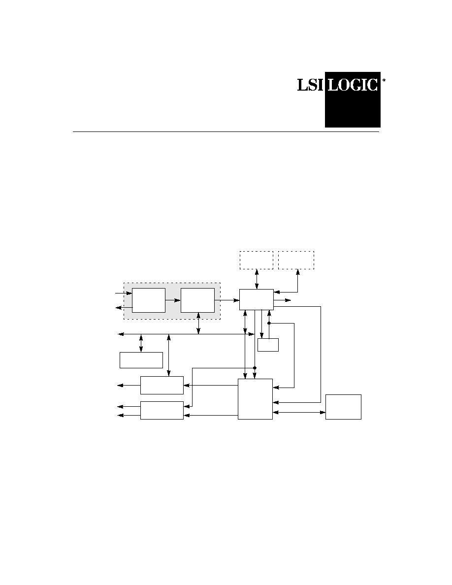
Figure 1
shows the
L64733/34 chipset satellite receiver implemented in a typical satellite
receiver set-top decoder box.
Figure 1
Block Diagram of Set-Top Decoder Box Using the L64733/34 Chipset
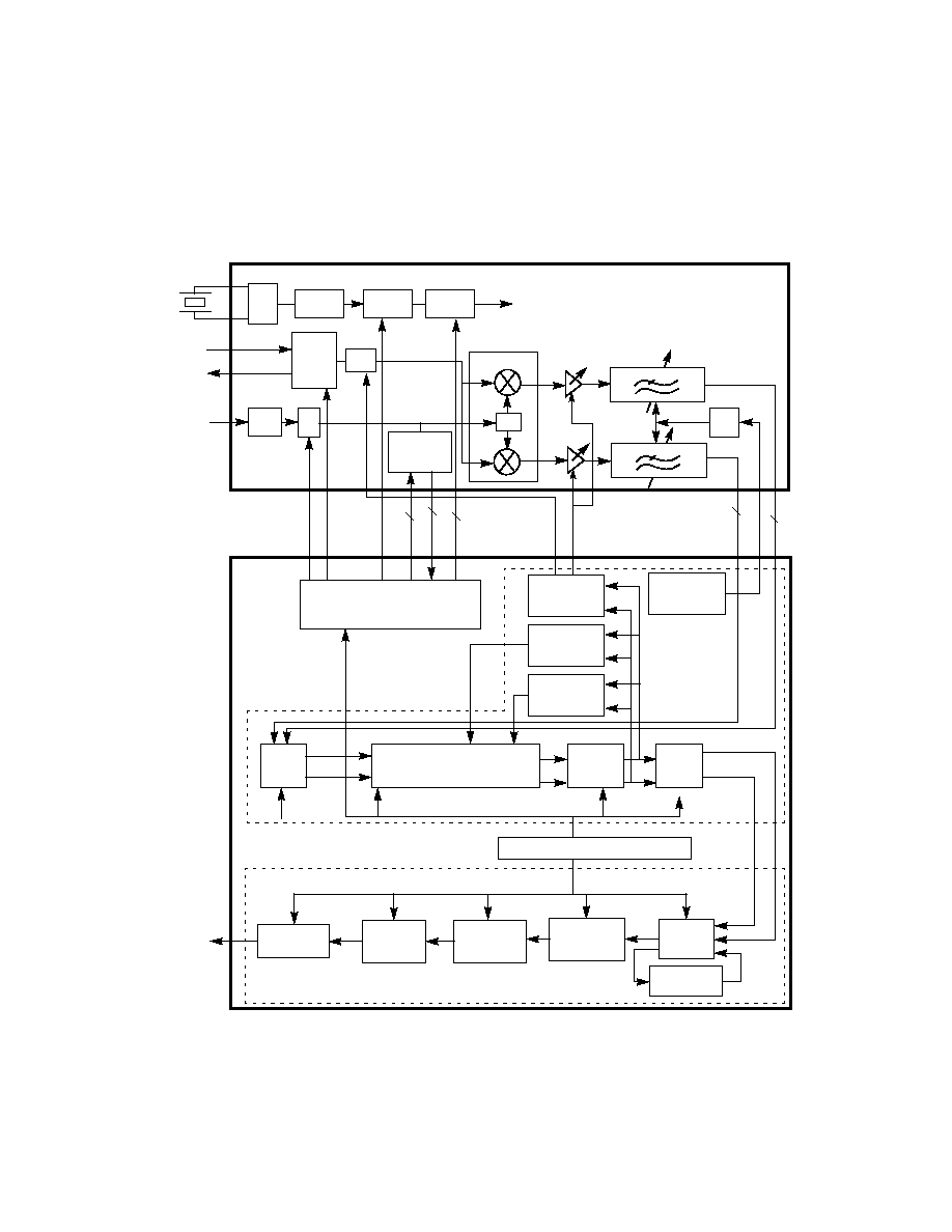
The L64733/34 chipset consists of the L64734 Satellite Receiver IC, the
L64733 Tuner IC, and an on-chip synthesizer.
Figure 2
shows a simplified
block diagram of this chipset.
CO
[7:0]
PCM
L64733
Transport
256K x 16
VCXO
256K x 64
DRAM
SDRAM
PAL / NTSC
NTSC
PAL
S-Video
L-Speaker
R-Speaker
27 MHz
Audio/Video PES
CCIR601VIDEO
PCM AUDIO
Encoder
Audio DAC
Satellite In
64/32
16
High-Speed
Port
8
Audio
Oversampling
Clock
/
/
8
/
8
/
3
/
2
/
Audio/Video
256K x 32
Demux
Decoder
Decryption
Engine
Optional
8
/
Microprocessor
L64733/L64734 Chipset
Optional
Microprocessor
Data and
Address Bus
L64734
RF Out
(Loop Through)

2
L64733/L64734 Tuner and Satellite Receiver Chipset
Figure 2
L64733/34 Simplified Block Diagram
The L64734:
∑
generates control signals for the L64733 synthesizer, using
frequency information programmed into the L64734 configuration
registers
∑
controls the programming of the low-pass filters on the L64733
∑
generates dual AGC control voltages for the two-stage automatic
gain control on the L64733 IC.
The L64733 Tuner IC directly down-converts the satellite signal from
L-band to baseband.
RF
RF Input
RF Output
Select
IOUT
QOUT
Dual ADC
Demodulator
Error
Correction
Descrambler
Microcontroller
Interface
Microcontroller
Host
Control
Modules for
MPEG Output
L64733
L64734
Control Signals
Synthesizer,
Baseband
Filter
Synthesizer
and Filter
Switch
Mixer,
Down-
Converter
L64733/L64734 Tuner and Satellite Receiver Chipset
3
Figure 3
shows a more detailed chipset block diagram.
Figure 3
Detailed Chipset Block Diagram
Filter
Matched
Filter
Carrier
Loop Control
AGC
Control
Timing Loop
Control
Output
Control
DEMI
DEMQ
1/T
Descrambler
Dual
ADC
Interpolator/Decimation
External Microcontroller Interface
Clk
(from L64734
on-chip PLL)
Xtal
Osc
Phase
RF In
RF Out
RF
Charge
Pump
Fc
90
∞
VCO
X2
Dual-
Tank
Circuit
PLLIN
FDOUB
MOD
PSOUT
CPG
A
GC1
INSEL
IOUT
QOUT
FLCLK
Synthesizer Control Module
L64734
L64733
Detect.
Filter
Control
Module
Amp
To External
Loop Filter
˜
by 8
Quadrature
Down-Converter
2
2
2
2
A
GC2
4≠7.26 MHz
Modulus
Prescaler
BPSK/QPSK
Demodulator
Microcontroller Data and Address Bus
Microcontroller Data and Address Bus
FEC Decoder Pipeline
Channel
Output
(MPEG-2
Transport
Stream)
Reed-
Solomon
Decoder
Convolutional
Deinterleaver
Reed-
Solomon
Synchronizer
Viterbi
Synchronizer
Viterbi
Decoder
Switch
2

4
L64733/L64734 Tuner and Satellite Receiver Chipset
The L64733 directly accepts the RF In L-Band signal input from the
satellite LNB feed. The L64733 handles a fully loaded raster of
transponder signals from 925 MHz to 2175 MHz. RF In is internally
matched to 75
, and except for a DC-blocking capacitor, requires no
matching network between the cable connector and the L64733 input
pins. The L64733 uses the L64734 INSEL signal to select the
appropriate RF function (Normal or Loop-Through mode).
The RF signal goes to a variable gain stage, which is controlled by the
L64734 AGC1 signal. The L64734 adjusts AGC1 in conjunction with
AGC2 to maximize the SNR of the RF signal while maintaining proper
levels at the baseband outputs (IOUT and QOUT). The signal then goes
to two mixers in the quadrature demodulator. The mixers are fed with
local oscillator signals that are offset by 90 degrees from one another.
The quadrature demodulator performs a direct frequency conversion of
the RF signal to baseband while splitting the signal into quadrature I and
Q signal paths.
The baseband signals pass through a pair of variable-gain amplifiers that
are controlled by the AGC2 pin, which, in turn is controlled by the
L64734. The signals are then filtered through a pair of 7th-order filters
for anti-aliasing. The filter shape is 7th-order Butterworth, followed by a
single-pole delay equalizer. The filter cut-off frequency, which is
controlled by the L64734 FLCLK signal, is related to the baud rate. The
filtered baseband output signals go to the differential output stages at
IOUTp, IOUTn, QOUTp and QOUTn.
The baseband outputs of the L64733 go to the L64734, where they are
digitized by the analog-to-digital converter (ADC). The outputs then go to
a BPSK/QPSK demodulator, where they are filtered. The demodulator
then sends them to the L64734 FEC decoder pipeline, which outputs an
MPEG-2 transport stream.
The frequency synthesizer functionality is split between the L64733 and
L64734. The Synthesizer Control Module resides on the L64734; it
generates control signals for the L64733 Tuner IC frequency synthesizer.
The Synthesizer Control Module also contains some of the
programmable counters that are part of the synthesizer feedback loop.
The L64733 contains many of the analog functions of the frequency
synthesizer, as well as the RF local oscillator and crystal reference
oscillator. Tuning oscillator signals are generated for the mixers in the

L64733/L64734 Tuner and Satellite Receiver Chipset
5
range from 925≠2175 MHz, with a 0.5 MHz step size when using a
4-MHz crystal reference. The on-chip VCO tuning frequency is 543 MHz
to 1088 MHz. To tune channels from 925≠1086 MHz, the L64734
disables the frequency doubler (X2 block) on the L64733. To tune
channels from 1086 MHz to 2175 MHz, the L64734 enables the
frequency doubler. The VCO requires an external resonant tank circuit,
which includes varactor diodes to vary the frequency of oscillation.
The VCO signal goes to the Prescaler block before it is passed to the
L64734 differentially through the PSOUTp and PSOUTn pins. The
L64734 MODp and MODn differential signals control the divider ratio for
the Prescaler block. The L64734 dynamically changes the divide ratio to
ensure that the tuning step size is not affected by the divider. The
L64734 contains programmable counters to further divide the signal in
frequency before the signal is fed back to the L64733 through the PLLINp
and PLLINn pins. The crystal reference oscillator frequency is divided by
eight, then fed to the phase detector. The phase detector generates a
current signal proportional to the difference in phase between PLLINp,
PLLINn, and the divided crystal frequency. A charge pump circuit (which
controls pins CP, FB) and an external transistor (to buffer the L64733
against the tuning voltage of 28 V) generate the current. The current is
filtered, fed through a discrete loop filter, and converted to a tuning
voltage that drives the external varactor diodes for the VCO tank circuit.
A complete frequency controlled loop is formed, and the VCO frequency
can be varied by changing the frequency divider ratios in the L64734
registers. See
Figure 7
on
page 22
for more details regarding the
external circuitry for the VCO, crystal oscillator, charge pump, tank
circuitry, and entire frequency-controlled loop.
The chipset provides maximum integration and flexibility for system
designers at a minimum cost. The number of external components
required to build a system is minimal because the synthesizer, variable
rate filters, and clock and carrier loops are all integrated into the two
devices.