 | –≠–ª–µ–∫—Ç—Ä–æ–Ω–Ω—ã–π –∫–æ–º–ø–æ–Ω–µ–Ω—Ç: LCBG10p | –°–∫–∞—á–∞—Ç—å:  PDF PDF  ZIP ZIP |

April 1998
1
Copyright © 1998 by LSI Logic Corporation. All rights reserved.
Bidirectional 3.3 V Universal LVD
Transceiver (G10TM)
Datasheet
LSI Logic's bidirectional transceiver for SCSI is used to transmit and
receive data on a SCSI-2, SCSI-3 10 MHz, SCSI-3 ULTRA, or SCSI-3
ULTRA-2 single-ended or differential bus. The bus operates at rates up
to 40 MHz, with a cable length up to 25 m and maximum stub lengths of
0.1 m. SCSI bus termination is assumed to be external to the SCSI
device.
This transceiver can operate with SCSI-2, SCSI-3 10-MHz interfaces,
SCSI-3 Fast-20, or SCSI-3 Fast-40 interfaces. Typically, the single-ended
or differential operating mode is controlled by a "DIFFSENSE" receiver,
a description of which is included in this datasheet. This transceiver is
implemented in G10 technology.
This transceiver conforms to the
Information Technology - SCSI-3
Parallel Interface Specification SPI-2 Project 1142D.
Figure 1
SCSI Bus Interface
FPO
SCSI
Host Adapter
2
Target Devices
PC or Workstation
3
4
5
14
15
16
Termi-
nation
Termi-
nation

2
Bidirectional 3.3 V Universal LVD Transceiver (G10)
Features and Benefits
Specifications
The following subsections provide the specifications for the SCSI
bidirectional universal LVD 3.3 V transceivers.
Figure 2
shows the schematic symbol for the bidirectional universal LVD
transceiver.
Complies with
SCSI-3 SPI-2 Parallel
Interface Specification
Complies with
the American National
Standard for Information Systems
SCSI-3 Fast-20
Reduces engineering effort of designing
an interconnect to SCSI bus
Has V/I characteristics that meet the
SCSI bus drive requirements
Provides for direct silicon interconnect
to a SCSI transmission line
On-chip 48 mA drivers
3.3 V V
DD
(5-volt-tolerant)
Bidirectional I/O transceiver that provides
maximum flexibility in I/O path design
Available in the G10 cell-based product
families (0.35-micron drawn gate length,
0.29-micron effective channel length)
Transfer rates up to 40 MHz
Active negation SE driver
Bidirectional 3.3 V Universal LVD Transceiver (G10)
3
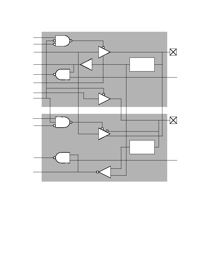
Figure 2
Bidirectional Universal LVD Transceiver Logic Diagram
TN
EN
ZI
A
POM
NEG
B
DIFF
TNDIFF
ENDIFF
POP
ZIDIFF
PIP
IOM
PIM
IOP
Single-Ended Portion
Input
Protection
Differential
Portion
Input
Protection
Signal -
Signal +
+
-
Name:
BDLVDSCSIF
Description:
SCSI 3.3 V bidirectional transceiver used with the SCSI-2,
SCSI-3 10 MHz, SCSI-3 FAST-20, and SCSI-3 FAST-40
Buses
Coding Syntax:
U(IOM, IOP, ZI, ZIDIFF, PORN, POP) =
BDLVDSCSIF (IOM, IOP, A, B, EN, NEG, TN, ENDIFF,
TNDIFF, PIM, PIP, DIFF, IDDTN, HTPLG)
Silicon Dimensions: 285.6
µ
m x 226.8
µ
m

4
Bidirectional 3.3 V Universal LVD Transceiver (G10)
Cell Placement Restrictions
The following cells are designed to be used with G10 technology:
pvdd2_lvdscsi: To supply vdd2
apvdd_lvdscsi: To supply analog V
DD
apvss_lvdscsi: To supply analog V
SS
pvdd_lvdscsi:
To supply 3.3 V to the I/O
pvss2_lvdscsi: To supply vss2
dvdd_lvdscsi:
Dummy cell for differential SCSI cells
dvddil_lvdscsi: Left dummy interface cell
dvddir_lvdscsi: Right dummy interface cell
The first five cells in this list supply vdd2, avdd, avss, 3.3 V I/O, and vss2
to the SCSI buffers. The dvdd_lvdscsi, dvddil_lvdscsi, and dvddir_lvdscsi
cells provide a protection diode between vddlvdscsi and vssio. Adhere to
the following guidelines when placing these cells:
1.
At least one dummy cell must be placed at both ends of the SCSI
section.
2.
There must be at least one pvdd_lvdscsi, apvdd_lvdscsi, and
apvss_lvdscsi cell per five SCSI buffers; one V
SS
per two SCSI
buffers.
Recommended Operating Conditions
Table 1
provides the recommended operating conditions for the
bidirectional SCSI I/O Transceiver.
Table 1
Recommended Operating Conditions
Symbol
Parameter
Minimum
Typical
Maximum
Unit
V
DD
DC Supply Voltage
3.14
3.3
3.46
V
T
j
Junction Temperature
0
30
125
∞C

Bidirectional 3.3 V Universal LVD Transceiver (G10)
5
Table 2
provides the loading characteristics for the control portion of the
bidirectional transceiver. Values are in standard loads.
Table 3
provides the AC timing for the bidirectional transceiver's input
portion. These specifications are valid only for the commercial operating
range: junction temperature = 0 ∞C to 125 ∞C, V
DD
= 3.3 V
±
5%.
Table 2
Bidirectional Universal LVD Transceiver's Loading Characteristic
1
A
B
EN
TN
ENDIFF TNDIFF
NEG
HTPLG
DIFF
IDDTN
PIM
PIP
3.5
1.2
0.8
1.5
2.2
3.1
0.9
0.9
9.8
5.5
13.9
1.6
1. One standard load = 0.0151775 pF.
Table 3
Bidirectional Universal LVD Transceiver's AC Delay
Characteristics for Transmitters (ns)
Delay Path
Output
Capacitance Load (pF)
15
50
85
100
A to IOM
tpLH
3.98
4.77
5.48
5.77
tpHL
3.79
4.58
5.19
5.42
tpZL
6.87
7.66
8.36
8.64
tpLZ
10.18
9.95
9.74
9.67
EN to IOM
tpZH
2.61
4.14
5.91
6.67
tpZL
6.93
7.72
8.42
8.70
tpLZ
10.20
9.97
9.76
9.69
tpHZ
1.49
1.49
1.49
1.49
TN to IOM
tpZH
2.41
4.19
5.96
6.72
tpZL
6.79
7.59
8.29
8.57
tpLZ
10.11
9.88
9.67
9.59
tpHZ
1.38
1.38
1.38
1.38
(Sheet 1 of 2)