The
Communications
Company
TM
O V E R V I E W
Central offices providing asymmetric digital subscriber line (ADSL) service are
seeking a digital subscriber line access multiplexer (DSLAM) solution that integrates
the largest number of ports per line card with lowest power consumption. DSLAM
providers are limited by the power dissipation of the ADSL transceiver (in
particular, the analog integrated circuits), and by the physical space occupied per
port. Addressing this need, LSI Logic developed SpeedREACH AC8200, a highly
integrated component containing eight complete analog front ends (AFEs) for
G.dmt (full-rate) or G.lite ADSL operation in a small 14 mm x 20 mm 128-pin
package, with a power dissipation of 150 mW per channel.
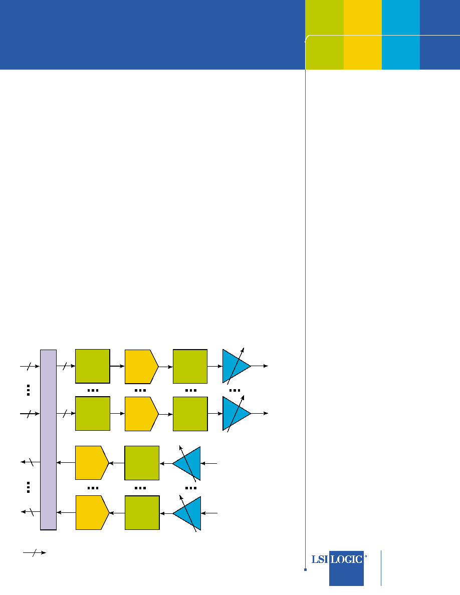
In the receive (RX) portion of the chip, the incoming analog differential
signals enter the chip at the RX1 In through RX8 In pins, respectively. The RX
analog signal path for each channel is partitioned into a continuous-time (CT)
section and an analog-digital converter (ADC). The CT section consists of a
programmable gain stage followed by a 4th-order low-pass RX filter,
implemented as a simple cascade of two 2nd-order low-pass structures. The 4th-
order filter may be set to either 138 kHz ADSL over POTS or to 276 kHz, for
ADSL over ISDN. The gain is set by the user by programming the appropriate
receive-gain (RXGAIN) register. The output of the filter is fed directly to the ADC,
which samples at 1.104 MS/s or 552 kS/s and outputs a 16-bit word.
SpeedREACH
TM
AC8200 -- Octal
ADSL Analog Front End for CO
F E A T U R E S
∑ ADSL CO AFE with eight full RX and
TX analog signal paths (excluding high-
voltage line drivers)
∑ Fully monolithic: only 1 precision resistor,
and decoupling capacitors required
∑ Compatible with ITU G.992.1 (G.dmt)
and G.992.2 (G.lite) standards
∑ Eight 14-bit linear 1.104 MS/s ADCs and
Eight 14-bit linear 4.416 MHz DACs
∑ Completely integrated RX/TX filters
∑ 4th-order low-pass filters for RX and TX
paths, with ±5% cutoff frequency accuracy
∑ Programmable digital TX high-pass
filter: up to 6th order
∑ RX channel: support for both 138 kHz
and 276 kHz (for ADSL over ISDN)
∑ TX channel: support for both 552 kHz
(G.lite) and 1.104 MHz (G.dmt)
∑ RX path programmable gain amplifiers
(PGAs): 44 dB of range
∑ TX path programmable attenuation
amplifiers (PAAs): 0 dB to ≠18 dB
∑ Entire RX channel linearity: 80 dB MTPR and
Entire TX channel linearity: 70 dB MTPR
∑ Low pincount digital interface for RX/TX
∑ Power: 1.2 W (8 channels fully
on, configured for full-rate ADSL --
i.e., 150 mW per channel)
TX HPF
Variable From
100kHz to
200kHz
DAC
4.4MHz
16
PAA
ADC
1.1MS/s/
552kS/s
RX1 In
Low-Noise PGA
G
RX LPF
138kHz/
276kHz
ADC
1.1MS/s/
552kS/s
RX8 In
Low-Noise PGA
RX LPF
138kHz/
276kHz
MCLK
35.328MHz
16
16
TX LPF
1.1MHz/
552kHz
TX1 Out
Digital
I/F
2
TX1
TX HPF
Variable From
100kHz to
200kHz
DAC
4.4MHz
16
PAA
TX LPF
1.1MHz/
552kHz
TX8 Out
2
TX8
1
1
RX1
RX8
Figure 1. Block diagram of the SpeedREACH AC8200.

The
Communications
Company
TM
SpeedREACH
TM
AC8200
In the transmit (TX) portion of the chip, for each channel, the incoming 2.2 MHz
16-bit digital word from the digital interface block is passed to a programmable
high-pass filter. This filter is a cascade of 3 biquads allowing up to a 6th-order
response. The filter internal implementation is designed to support typical responses
(Butterworth, Chebyshev, etc.) over a cut-off frequency range between 100 kHz and
200 kHz. The coefficients are user-programmable to allow optimization for a
particular application or line condition. The output of the digital filter is fed to the
digital-analog converter (DAC) at a 4.416 MHz update rate. The DAC output is re-
sampled (de-glitched) and is passed to the CT section comprising a 4th-order low-
pass filter followed by a programmable attenuation amplifier (PAA). The attenuation
is set by the user by programming the appropriate transmit-gain (TXGAIN) register.
The outputs of the PAAs appear at the TX1 Out through TX8 Out pins, respectively,
and can drive an AC-coupled load of 2 k
W with maximum level of ±2.5 V or +5 V
peak-to-peak differential.
The digital interface for the primary TX data consists of a 2-bit stream at
17.6 MHz, to support an overall 2.208 MHz incoming data rate; and for the
primary RX data, a 1-bit stream at 17.6 MHz, to support up to 1.104 MHz
outgoing data rate.
The chip requires a single low-jitter 35.328 MHz clock to be applied at the
master clock (MCLK) pin. All clock generation is performed internally and all
converter and sample and hold (S/H) clocks in both RX and TX paths are directly
derived from MCLK.
A 4-wire serial port provides a simple DSP interface. The serial port is used
to modify internal register values, which in turn control attenuation/gain settings,
filter bandwidths and the power down of individual blocks. The chip is powered
off a +5 V supply while all digital I/Os run off a +3.3 V supply. The AC8200
is available in a 128-pin LQFP plastic package. The operating temperature
range is between -40∞ C and +85∞ C.
For more information please call:
LSI Logic Corporation
North American Headquarters
Milpitas, CA
Tel: 800 574 4286
LSI Logic Europe Ltd.
European Headquarters
United Kingdom
Tel: 44 1344 426544
Fax: 44 1344 481039
LSI Logic KK Headquarters
Tokyo, Japan
Tel: 81 3 5463 7165
Fax 81 3 5463 7820
LSI Logic web site
www.lsilogic.com
LSI Logic logo design, is a registered trademark
and SpeedREACH is a trademark of LSI Logic
Corporation. All other brand and product names
may be trademarks of their respective companies.
LSI Logic Corporation reserves the right to make
changes to any products and services herein at any
time without notice. LSI Logic does not assume any
responsibility or liability arising out of the
application or use of any product or service
described herein, except as expressly agreed to in
writing by LSI Logic; nor does the purchase, lease,
or use of a product or service from LSI Logic
convey a license under any patent rights,
copyrights, trademark rights, or any other of the
intellectual property rights of LSI Logic or of third
parties.
Copyright ©2001 by LSI Logic Corporation.
All rights reserved.
Order No. R20027
101.1k.JG.LT - Printed in USA