Specifications subject to change without notice.
∑
North America: 1-800-366-2266
Visit www.macom.com for complete contact and product information.
Typical Performance @ 25∞C
Guaranteed
Characteristics
Typical
0
∞
∞
∞
∞
to 50
∞
∞
∞
∞
C
-54
∞
∞
∞
∞
to +85
∞
∞
∞
∞
C
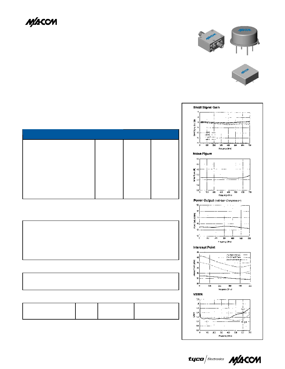
Frequency
Small Signal Gain (min.)
Gain Flatness (max.)
Reverse Isolation
Noise Figure (max.)
Power Output @ 1 dB comp. (min.)
IP3
IP2
Second Order Harmonic IP
VSWR Input / Output (max.)
DC Current @
Absolute Maximum Ratings
Storage Temperature
Max. Case Temperature
Max. DC Voltage
Max. Continuous RF Input Power
Max. Short Term RF Input Power (1 minute max.)
Max. Peak Power (3
µ
sec max.)
"S" Series Burn-in Temperature (Case)
Thermal Data: V
cc
=
Thermal Resistance
jc
Transistor Power Dissipation P
d
Junction Temperature Rise Above Case T
jc
Outline Drawings
Package TO-8 Surface Mount SMA Connectorized
Figure
Model
∑ LOW NOISE FIGURE: 3.2 dB (TYP.)
∑ HIGH EFFICIENCY: 31 mA (TYP.) at +5 Vdc
∑ HIGH OUTPUT POWER: +12.5 dBm (TYP.)
A611/SMA611
2000 TO 6000 MHz
CASCADABLE AMPLIFIER
Specifications (Rev. Date: 2/03)*
Measured in a 50-ohm system at +5 Vdc Nominal. All connectorized products are guaranteed over a
temperature range of 0∞ to +50∞C.
BG
AA
CE
2-700 MHz
15.0 dB
±0.2 dB
20 dB
3.2 dB
12.5 dBm
+24 dBm
+30 dBm
+36 dBm
1.4:1 / 1.4:1
31 mA
5-600 MHz
14.0 dB
±0.6 dB
10.5 dBm
3.8 dB
11.0 dBm
1.9:1 / 1.9:1
36 mA
1.8:1 / 1.8:1
34 mA
5-600 MHz
13.5 dB
±0.8 dB
4.5 dB
-62∞ to +125∞C
125∞C
+10 Volts
+10 dBm
50 mW
0.5 W
125∞C
185∞C/W
0.123 W
23∞C
A611
SMA611
CA611
5 Volts (max.)
5 Vdc
*