V 2.00
F e a t u r e s
Low Noise Figure: 1.15 dB
High Gain: 27 dB
Low Power Consumption: 3 to 5 V, 20 mA
High Dynamic Range
Low Cost SOIC 8 Plastic Package
D e s c r i p t i o n
M/A-COM's AM50-0002 is a high perf o rmance GaAs
MMIC low noise amplifier in a low cost SOIC 8-lead sur-
face mount plastic package. The AM50-0002 employs a
monolithic 3-stage self-bias design and a simple extern a l
matching network to obtain minimum noise figure. It can
be biased using 3- or 5-volt supplies.
The AM50-0002 is ideally suited for use where low noise
f i g u re, high gain, high dynamic range and low power
consumption are re q u i red. Typical applications include
receiver front ends in the Global Positioning System
(GPS) market, as well as standard gain blocks, buff e r
amps, driver amps and IF amps in both fixed and
portable systems.
M/A-COM's AM50-0002 is fabricated using a mature 0.5-
m i c ron gate length GaAs process. The process feature s
full passivation for increased perf o rmance re l i a b i l i t y .
Parameter
Units
Min.
Typ.
Max.
Gain
dB
25
27
29
Noise Figure
dB
1.15
1.4
Input VSWR
2.0:1
Output VSWR
1.5:1
Output1 dB Compression
dBm
1
Input IP3
dBm
-14
Reverse Isolation
dB
48
Bias Current
mA
15
20
25
1. See following pages for 3-volt data.
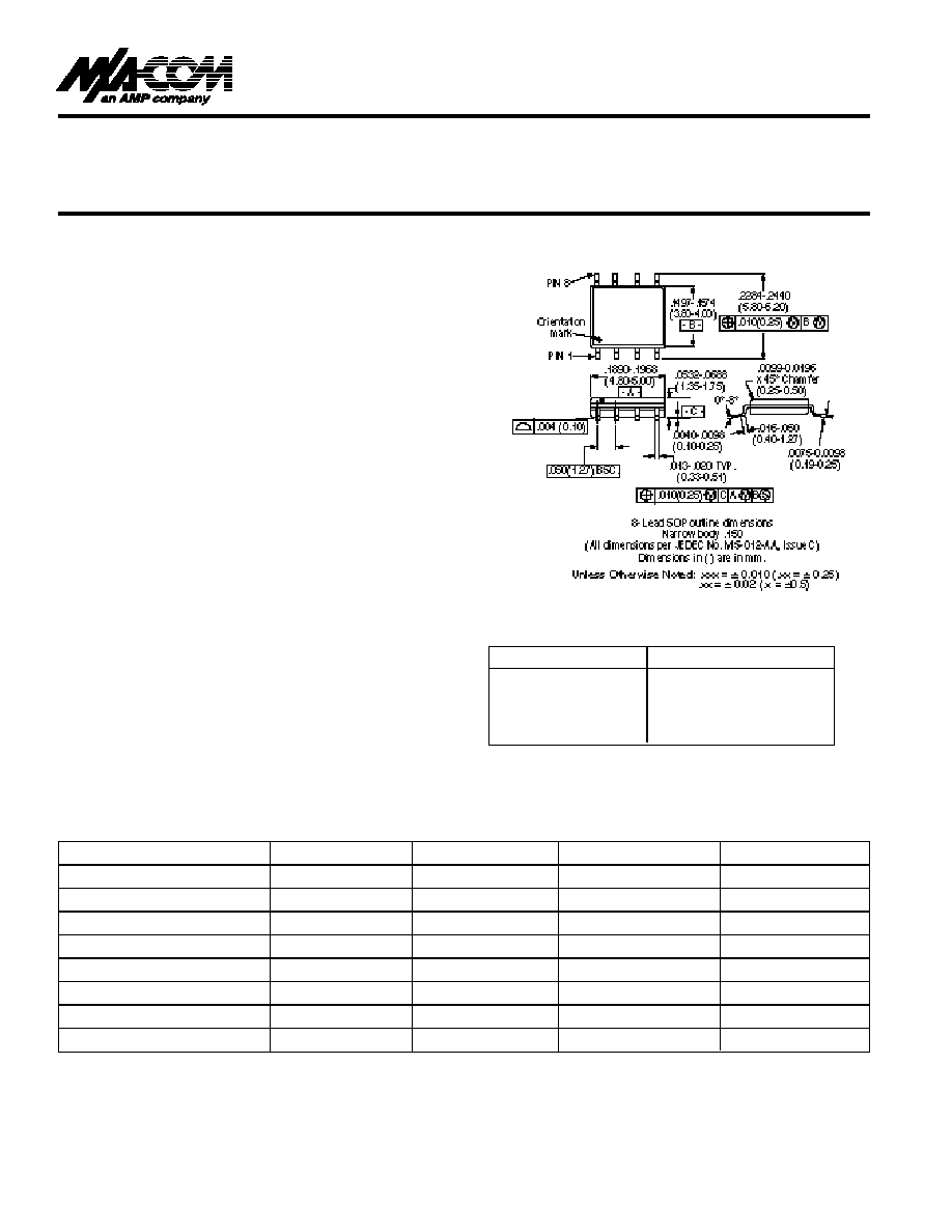
Low Noise Amplifier
1.575 GHz
AM50-0002
Electrical Specifications
1
T
A
= +25∞C, Z
0
= 50
, V
DD
= +5V, P
IN
= -35 dBm, f= 1.575 GHz
SO-8
q
q
q
q
q
Part Number
Package
AM50-0002
SOIC 8-Lead Plastic
AM50-0002TR
Forward Tape and Reel*
AM50-0002RTR
Reverse Tape and Reel*
AM50-0002SMB
Designer's Kit
Ordering Information
*
If specific reel size is required, consult factory for part number
assignment.
V 2.00
Absolute Maximum Ratings
1
Parameter
Absolute Maximum
V
DD
+10 VDC
Input Power
+17 dBm
Channel Temperature
2
+150∞C
Operating Temperature
-40∞C to 85∞C
Storage Temperature
-65∞C to 150∞C
1. Operation of this device outside these limits may cause
permanent damage.
2. Typical thermal resistance ( jc) = +165∞C/W
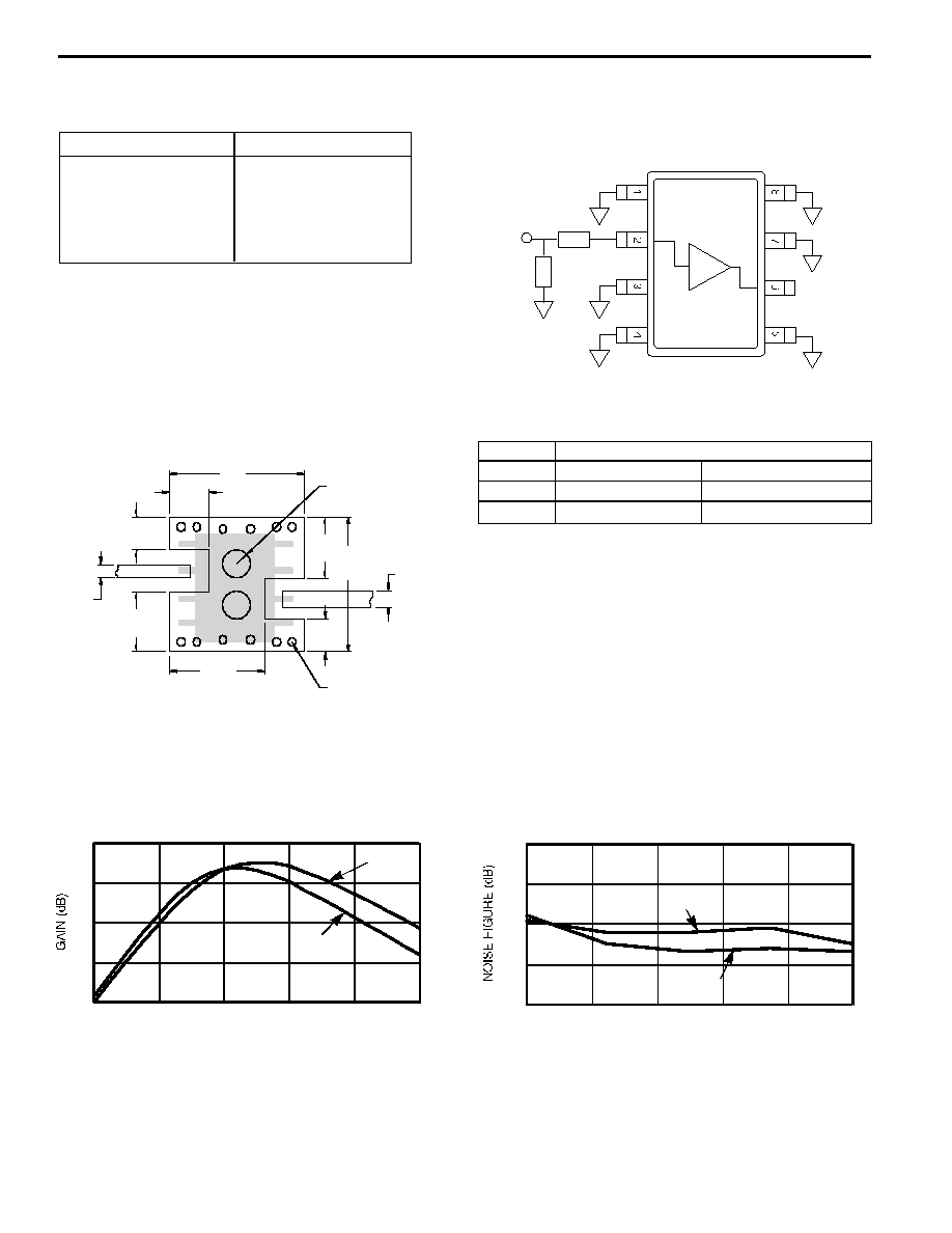
Low Noise Amplifier
AM50-0002
Typical Performance
Functional Diagram
RF OUT, V
DD
GND
GND
GND
GND
GND
GND
RF IN
T1
T2
FREQUENCY (GHz)
FREQUENCY (GHz)
GAIN
v s
F R E QU E N C Y, TA = +25∞C
NOISE FIGURE
v s
F R E QU E N C Y, TA = +25∞C
Recommended PCB Configuration
Frequency = 1.575 GHz
Impedance
Electrical Length
T1
57.2
36.0∞
T2
82.7
16.2∞
3. Pins 1, 3, 4, 5, 7 and 8 must be RF and DC grounded as shown.
4. Pin 2 is the RF input and must be connected to the simple matching
network shown.
5. Pin 6 is the RF output. V
DD
is also applied on pin 6.
0.030
(0.76)
2X R 0.025 (0.64)
PLATED THRU
12 X R 0.008 (0.20)
PLATED THRU
0.024
(0.61)
0.060
(1.52)
0.109
(2.77)
0.060
(1.52)
0.172
(4.37)
0.244
(6.20)
0.072
(1.83)
0.112
(2.84) 0.245
(6.22)
RF IN
RF OUT
Dimensions in inches (mm)
FR-4 circuit board, thickness = 0.016 inches (0.41)
28
26
24
22
20
1.3
1.4
1.5
1.6
1.7
1.8
5 V
3 V
1.4
1.3
1.2
1.1
1.0
1.50
1.52
1.54
1.56
1.58
1.60
3 V
5 V
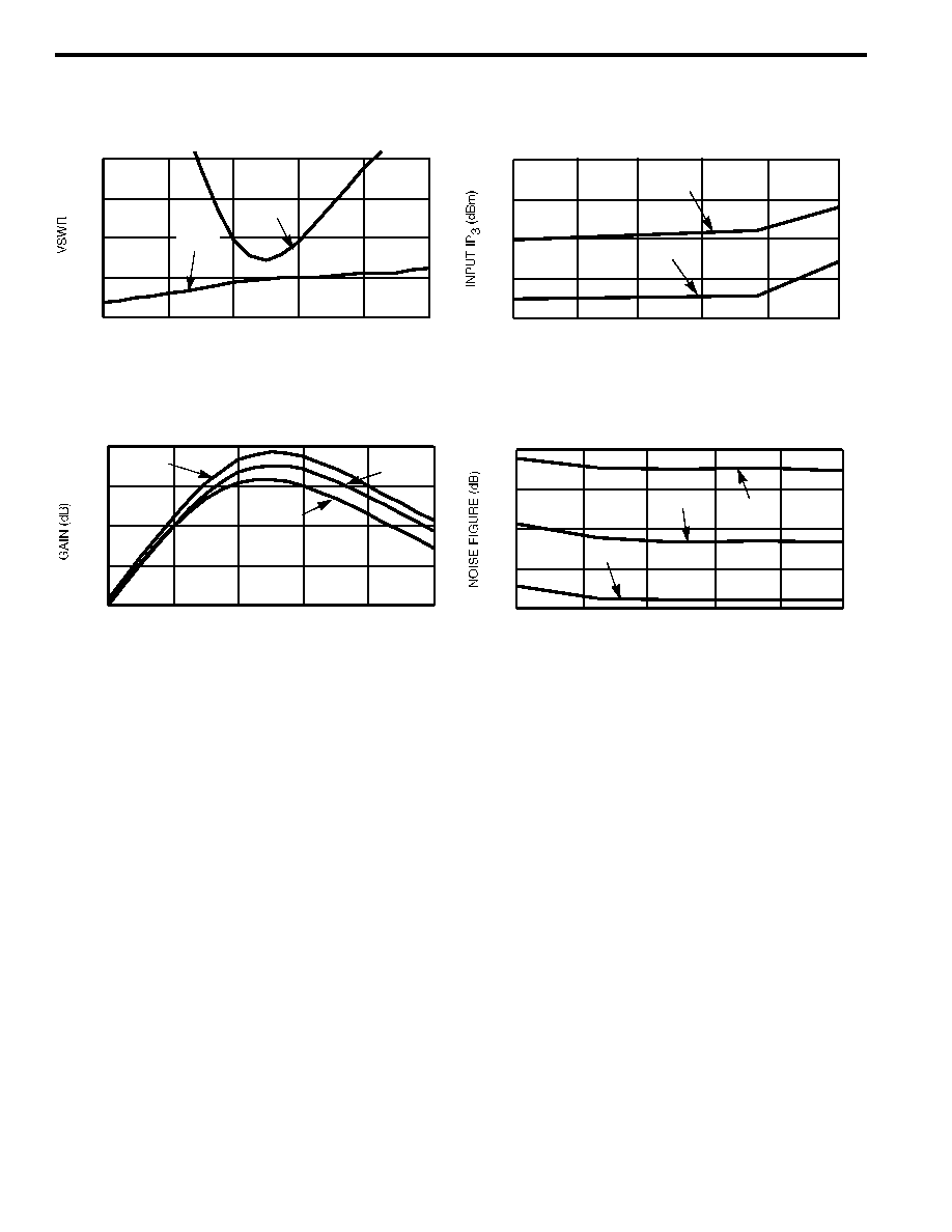
V 2.00
Low Noise Amplifier
AM50-0002
FREQUENCY (GHz)
FREQUENCY (GHz)
VSWR
v s
F R E QUENCY @ 5 V, TA = +25∞C
INPUT IP3
v s
F R E QU E N C Y, TA = +25∞C
FREQUENCY (GHz)
FREQUENCY (GHz)
GAIN
v s
F R E QUENCY @ 5 V
NOISE FIGURE
v s
F R E QUENCY @ 5 V
3.0
2.5
2.0
1.5
1.0
1.3
1.4
1.5
1.6
1.7
1.8
I n p u t
O u t p u t
28
26
24
22
20
1.3
1.4
1.5
1.6
1.7
1.8
- 4 0 ∞ C
+ 8 5 ∞ C
+ 2 5 ∞ C
-12
-13
-14
-15
-16
1.50
1.52
1.54
1.56
1.58
1.60
3 V
5 V
1.6
1.4
1.2
1.0
0.8
1.50
1.52
1.54
1.56
1.58
1.60
+ 8 5 ∞ C
+ 2 5 ∞ C
- 4 0 ∞ C
Additional information is available in Application Note M540,
"M/A-COM GaAs MMIC LNA SOIC-8 Platform."