Low Noise Amplifier
1.575 GHz
AM50-0002
1
V8
M/A-COM Inc. and its affiliates reserve the right to make changes to the
product(s) or information contained herein without notice. M/A-COM makes
no warranty, representation or guarantee regarding the suitability of its
products for any particular purpose, nor does M/A-COM assume any liability
whatsoever arising out of the use or application of any product(s) or
information.
∑ North America Tel: 800.366.2266 / Fax: 978.366.2266
∑ Europe Tel: 44.1908.574.200 / Fax: 44.1908.574.300
∑ Asia/Pacific Tel: 81.44.844.8296 / Fax: 81.44.844.8298
Visit www.macom.com for additional data sheets and product information.
Features
∑ Low Noise Figure: 1.15 dB
∑ High Gain: 27 dB
∑ Low Power Consumption: 5V, 20 mA
∑ High Dynamic Range
∑ SOIC-8 Package
Description
M/A-COM's AM50-0002 is a high performance GaAs
MMIC low noise amplifier in a SOIC 8-lead surface
mount plastic package. The AM50-0002 employs a
monolithic 3-stage self-bias design and a simple
external matching network to obtain minimum noise
figure.
The AM50-0002 is ideally suited for use where low
noise figure, high gain, high dynamic range and low
power consumption are required. Typical
applications include receiver front ends in the Global
Positioning System (GPS) market, as well as
standard gain blocks, buffer amps, driver amps, and
IF amps in both fixed and portable systems.
M/A-COM'S AM50-0002 is fabricated using a mature
0.5-micron gate length GaAs process. The process
features full passivation for increased performance
reliability.
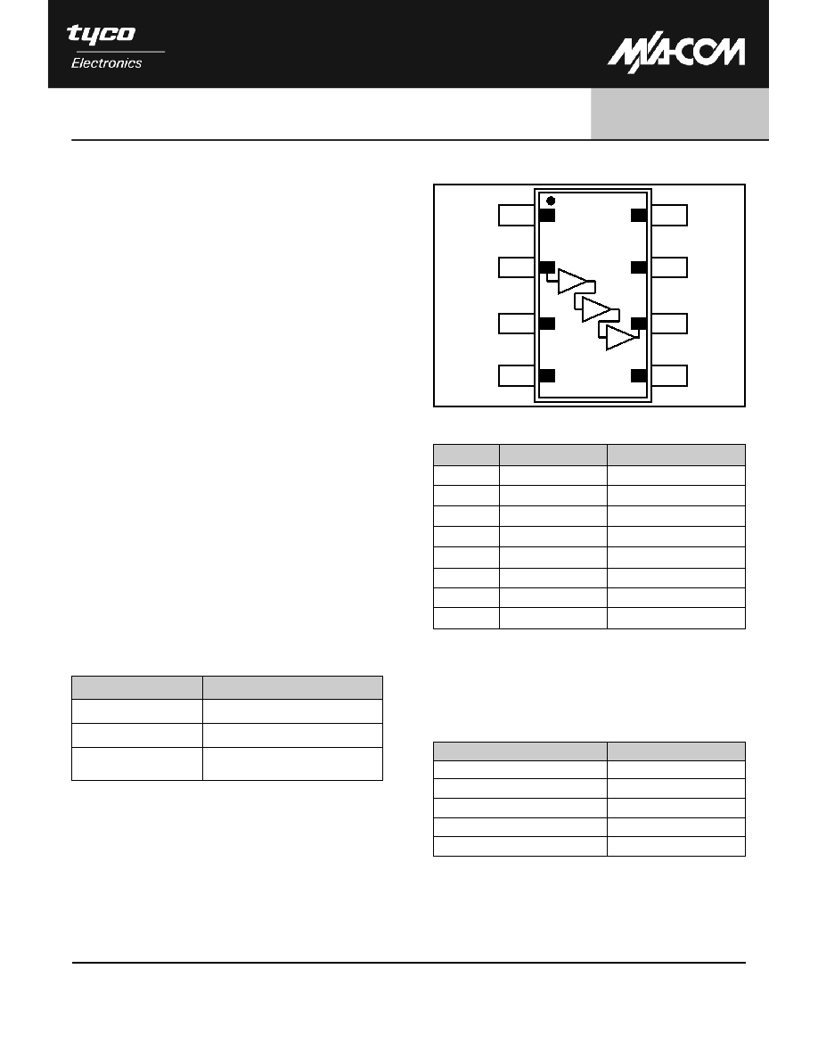
Functional Diagram
GND
RF IN
GND
RF OUT
GND
GND
GND
GND
GND
RF IN
GND
RF OUT
GND
GND
GND
GND
Ordering Information
Part Number
Package
AM50-0002
Bulk Packaging
AM50-0002TR-3000
3000 piece reel
AM50-0002SMB
Sample Test Board
(Includes 5 Samples)
Note: Reference Application Note M513 for reel size
information.
Absolute Maximum Ratings
4,5
Parameter
Absolute Maximum
V
DD
+10 VDC
Input Power
17 dBm
Channel Temperature
6
+150 ∞C
Operating Temperature
-40 ∞C to +85 ∞C
Storage Temperature
-65 ∞C to +150 ∞C
4. Exceeding any one or combination of these limits may cause
permanent damage to this device.
5. M/A-COM does not recommend sustained operation near
these survivability limits.
6. Typical thermal resistance (jc) = +165 ∞C/W
Pin No.
Pin Name
Description
1
GND
Ground
2
RF IN
RF Input
3
GND
Ground
4
GND
Ground
5
GND
Ground
6
RF OUT
RF Output, V
DD
7
GND
Ground
8
GND
Ground
Pin Configuration
1,2,3
1. Pins 1, 3, 4, 5, 7, and 8 must be RF and DC grounded (see
Recommended PCB Configuration).
2. Pin 2 is the RF input and must be connected to the simple
matching network shown in the Application Schematic.
3. Pin 6 is the RF output. V
DD
is also applied on Pin 6.

Low Noise Amplifier
1.575 GHz
AM50-0002
2
V8
M/A-COM Inc. and its affiliates reserve the right to make changes to the
product(s) or information contained herein without notice. M/A-COM makes
no warranty, representation or guarantee regarding the suitability of its
products for any particular purpose, nor does M/A-COM assume any liability
whatsoever arising out of the use or application of any product(s) or
information.
∑ North America Tel: 800.366.2266 / Fax: 978.366.2266
∑ Europe Tel: 44.1908.574.200 / Fax: 44.1908.574.300
∑ Asia/Pacific Tel: 81.44.844.8296 / Fax: 81.44.844.8298
Visit www.macom.com for additional data sheets and product information.
Electrical Specifications: T
A
= +25∞C, V
DD
= +5 V, Z
0
= 50
Parameter
Test Conditions
Units
Min.
Typ.
Max.
Gain
F = 1.575 GHz, P
IN
= -35 dBm
dB
25
27
29
Noise Figure
F = 1.575 GHz, P
IN
= -35 dBm
dB
-
1.15
1.4
Input VSWR
F = 1.575 GHz, P
IN
= -35 dBm
Ratio
-
2.0:1
-
Output VSWR
F = 1.575 GHz, P
IN
= -35 dBm
Ratio
-
1.5:1
-
Output P1dB
F = 1.575 GHz
dBm
-
1
-
Input IP
3
F = 1.575 GHz, P
IN
= -35 dBm
dBm
-
-14
-
Reverse Isolation
F = 1.575 GHz, P
IN
= -35 dBm
dB
-
48
-
Bias Current
--
mA
15
20
25
Frequency = 1.575 GHz
Impedance
Electrical Length
T1
57.2
36.0∞
T2
82.7
16.2∞
SOIC-8
Recommended PCB Configuration
Dimensions in inches (mm).
Application Schematic
1
2
3
4
8
7
6
5
GND
GND
GND
GND
GND
GND
T1
RF IN
T2
RF OUT, V
DD

Low Noise Amplifier
1.575 GHz
AM50-0002
3
V8
M/A-COM Inc. and its affiliates reserve the right to make changes to the
product(s) or information contained herein without notice. M/A-COM makes
no warranty, representation or guarantee regarding the suitability of its
products for any particular purpose, nor does M/A-COM assume any liability
whatsoever arising out of the use or application of any product(s) or
information.
∑ North America Tel: 800.366.2266 / Fax: 978.366.2266
∑ Europe Tel: 44.1908.574.200 / Fax: 44.1908.574.300
∑ Asia/Pacific Tel: 81.44.844.8296 / Fax: 81.44.844.8298
Visit www.macom.com for additional data sheets and product information.
Typical Performance
Gain, T
A
= +25∞C
Input IP
3
,
T
A
= +25∞C
Noise Figure over Temperature
Noise Figure, T
A
= +25∞C
VSWR, T
A
= +25∞C
20
22
24
26
28
1.3
1.4
1.5
1.6
1.7
1.8
Frequency (GHz)
Gain over Temperature
0.8
1.0
1.2
1.4
1.6
1.50
1.52
1.54
1.56
1.58
1.60
Frequency (GHz)
0.8
1.0
1.2
1.4
1.6
1.50
1.52
1.54
1.56
1.58
1.60
+25∞C
-40∞C
+85∞C
Frequency (GHz)
-16
-15
-14
-13
-12
1.50
1.52
1.54
1.56
1.58
1.60
Frequency (GHz)
1.0
1.5
2.0
2.5
3.0
1.3
1.4
1.5
1.6
1.7
1.8
Input
Output
Frequency (GHz)
20
22
24
26
28
1.3
1.4
1.5
1.6
1.7
1.8
+25∞C
-40∞C
+85∞C
Frequency (GHz)