Specifications Subject to Change Without Notice.
M/A-COM Inc.
1
North America: Tel. (800) 366-2266
Asia/Pacific: Tel. +81 3 3226-8761
Europe:
Tel. +44 (1344) 869-595
Fax (800) 618-8883 Fax +81 3 3226-8769
Fax +44 (1344) 300 020
Preliminary Release
1.2 W High Efficiency Power Amplifier
800 - 960 MHz
AM52-0001
V1.00
Features
∑
SOIC-8 Thermally Efficient Plastic Package
∑
+30.8 dBm Typical Power Out
∑
Greater than 50% Typical Power Added Efficiency
∑
21 dB typical Power Gain
∑
Flexible External Output Matching
Description
M/A-COM's AM52-0001 is a GaAs power amplifier in a thermally
efficient low cost SOIC-8 plastic package. The AM52-0001 is
designed for high efficiency 1.2 W output power and 21 dB of
associated gain in the 800-960 MHz frequency band. The
AM52-0001 is unconditionally stable in both small and large signal
operation. It features flexible biasing for improved dynamic range
and off-chip matching for improved efficiency and flexibility.
The AM52-0001 is specifically designed for high efficiency final
output power amplification in FM, GFSK and FSK type systems,
such as AMPS, ETACS, NTACS, CT1, CDPD and ISM.
M/A-COM's AM52-0001 is fabricated using a mature 0.5 micron
gate length GaAs MESFET power process. The process features
full passivation for increased performance and reliability. The
AM52-0001 can be used with standard automated SMT assembly
equipment (See M/A-COM application note M558).
SOIC-8P
.004 (.10)
.050 (1.27)
M
S
M
B
A
C
.010 (.25)
-A-
-C-
-B-
.010(.25)
B
CHAMFER
.1497/.1574
(3.80/4.00)
.2284/.2440
(5.80/6.20)
.1890/.1968
(4.80/5.00)
.013/.020 (8 PL)
(.33/.51)
.0532/.0688
(1.35/1.75)
M
M
Ordering Information
Part Number
Package
AM52-0001
SOIC-8 Lead Plastic
AM52-0001TR
Forward Tape and Reel *
AM52-0001SMB
Designer's Kit
* If specific reel size is required, consult factory for part number
assignment.
Electrical Specifications:
V
D1
= V
D2
= 4.8V
±
±
5%, T
A
= +25
∞
∞
C, Freq. = 824-849 MHz, V
GG
= V
G2
= V
G1
adjusted for 150 mA quiescent
drain Current.
Parameter
Test Conditions
Units
Min.
Typ.
Max.
Linear Gain
Pin
-20 dBm
dB
29
Output Power
Pin = 10 dBm
dBm
30.8
Power Gain
dB
21
Power Added Efficiency
%
55
Second Harmonic
dBc
-30
Third Harmonic
dBc
-50
Noise Power1
dBm
-92
Stability2
VSWR
10:1
Load Mismatch3
VSWR
10:1
Gate Current
mA
5
Adjustable Power Control (APC)
V
D1
= 0
4.8V V
D2
= 4.8 V
dB
27
1. Noise power (30 KHz RBW), 45 MHz above T
X
Freq range, measured under rated output power conditions.
2. Parasitic Oscillation defined as any spurious output less than 60 dBc with respect to desired signal level. Measured with nominal Pin and an output
VSWR of 10:1 any phase, V
DD
= 4.8 V.
3. No permanent degradation with nominal Pin and an output VSWR of 10:1 at any phase (360
∞
rotation in 10 sec.) with V
DD
up to 6V. .
1.2 W High Efficiency Power Amplifier
AM52-0001
V1.00
Specifications Subject to Change Without Notice.
2
M/A-COM Inc.
North America: Tel. (800) 366-2266
Asia/Pacific: Tel. +81 3 3226-8761
Europe:
Tel. +44 (1344) 869-595
Fax (800) 618-8883 Fax +81 3 3226-8769
Fax +44 (1344) 300 020
Absolute Maximum Ratings
1
Parameter
Absolute Maximum
Input Power
2
+23 dBm
Operating Voltage
2
V
DD
= + 10 Volts
V
GG
= - 6 Volts
Junction Temperature
3
+150
∞
C
Storage Temperature
-65
∞
C to +150
∞
C
Operating Temperature
-40
∞
C to +85
∞
C
1. Exceeding any one or combination of these limits may cause
permanent damage.
2. Ambient Temperature (T
A
) = + 25
∞
C
3. See temperature derating curve.
Pin Configuration
Pin No.
Pin Name
Description
1
V
G1
Negative supply voltage, First stage
2
RF IN
RF Input of the amplifier
3
GND
DC and RF Ground
4
V
D1
Positive supply voltage, First stage
5
V
G2
Negative supply voltage, First stage
6
GND
DC and RF Ground
7
RF OUT
RF Output of the amplifier
8
V
D2
Positive supply voltage, Second stage
9
Puck
DC and RF Ground
Recommended PCB Configuration
Layout View (AMPS 824-849 MHz)
0.47" (T1)
0.25" (T2)
C9
C8
C1
C6
C10
C3
C7
C11
C2
C4
C5
Functional Block Diagram
(AMPS 824-849 MHz)
1
2
4
3
8
7
5
6
C 1
C 2
C 3
C 4
C 5
C 6
C 7
C 8
C 9
C 1 1
R F O U T
R F IN
V D 1
V D 2
V G 2
V G 1
C 1 0
T 1
T 2
9
External Circuitry Parts List
(AMPS 824-849 MHz)
Part
Value
Purpose
C1 - C3
220 pF
By-Pass
C4 - C7
0.1 uF
By-Pass
C8
8 pF
Power Tuning
C9, C10
56 pF
DC Block
C11
1.0 uF
By-Pass
T1
0.470"
Matching Transmission
T2
0.250"
Lines (50
)
1.) The recommended layout is specifically for the AMPS application. It
shows EIA code size 0603 standard SMT capacitors with the exception of
C11 which is a EIA code size 3528
2.) The location of C9, C10 and C11 is not critical to the performance of
the amplifier.
Cross Section View
RF Traces + Components
RF Ground
DC Routing
Customer Defined
The PCB dielectric between RF traces and RF ground layers should
be chosen to reduce RF discontinuities between 50
lines and
package pins. M/A-COM recommends an FR-4 dielectric thickness
of 0.008"(0.2 mm) yielding a 50
line width of 0.015"(0.38 mm).
The recommended metalization thickness is 1 oz. copper and ground
metalization thickness is 2 oz.. Shaded traces are vias to DC
Routing layer and traces on DC Routing layer.
Biasing Procedure
The AM52-0001 requires that V
GG
bias be applied prior to ANY
V
DD
bias. Permanent damage will occur if this procedure is not
followed. All FETs in the PA will draw IDSS and damage internal
circuitry. Resistance added in seiries with V
g1
and V
g2
may degrade
performance.
1.2 W High Efficiency Power Amplifier
AM52-0001
V1.00
Specifications Subject to Change Without Notice.
M/A-COM Inc.
3
North America: Tel. (800) 366-2266
Asia/Pacific: Tel. +81 3 3226-8761
Europe:
Tel. +44 (1344) 869-595
Fax (800) 618-8883 Fax +81 3 3226-8769
Fax +44 (1344) 300 020
Typical Power Data (AMPS 824 - 849 MHz)
Test Conditions (unless otherwise noted) : TRoom = +25
∞
C, TCold = -40
∞
C, THot = +85
∞
C, Pin = 10 dBm, Freq. = 835 MHz, V
DD
= V
D1
= V
D2
= 4.8V and
V
GG
= V
G1
= V
G2
adjusted for 150 mA total quiescent drain current. External output matching circuitry is optimized for the 824 - 849 MHz AMPS
application.
OUTPUT POWER VS INPUT POWER
15
19
23
27
31
35
-13 -11
-9
-7
-5
-3
-1
1
3
5
7
9
11
13
Pin (dBm)
Pout (dBm)
Cold
Room
Hot
PAE VS INPUT POWER
0
10
20
30
40
50
60
70
-13 -11
-9
-7
-5
-3
-1
1
3
5
7
9
11
13
Pin (dBm)
PAE (%)
Room
Hot
Cold
DRAIN CURRENTS VS INPUT POWER
0
10
20
30
40
50
-13 -11 -9
-7
-5
-3
-1
1
3
5
7
9
11
13
Pin (dBm)
Id1 (mA)
0
200
400
600
800
1000
Id2 (mA)
Hot
Room
Cold
GAIN VS INPUT POWER
15
19
23
27
31
35
-13 -11
-9
-7
-5
-3
-1
1
3
5
7
9
11
13
Pin (dBm)
Gain (dB)
Cold
Room
Hot
GATE CURRENT VS INPUT POWER
-5
-4
-3
-2
-1
0
-13
-11
-9
-7
-5
-3
-1
1
3
5
7
9
11
13
Pin (dBm)
IG2 (mA)
Room
Hot
Cold
OUTPUT POWER VS FREQUENCY
29.5
30.5
31.5
32.5
33.5
800
810
820
830
840
850
860
870
880
890
900
Frequency (MHz)
Pout (dBm)
Cold
Hot
Room
1.2 W High Efficiency Power Amplifier
AM52-0001
V1.00
Specifications Subject to Change Without Notice.
4
M/A-COM Inc.
North America: Tel. (800) 366-2266
Asia/Pacific: Tel. +81 3 3226-8761
Europe:
Tel. +44 (1344) 869-595
Fax (800) 618-8883 Fax +81 3 3226-8769
Fax +44 (1344) 300 020
Typical Power Data cont'd
PAE VS FREQUENCY
50
52
54
56
58
60
62
64
66
68
70
800
810
820
830
840
850
860
870
880
890
900
Frequency (MHz)
PAE (%)
Cold
Hot
Room
OUTPUT POWER, GAIN, AND PAE VS V
DD
15
17
19
21
23
25
27
29
31
33
35
3
3.5
4
4.5
5
5.5
6
6.5
Vdd (V)
Pout (dBm) & Gain (dB)
55
56
57
58
59
60
61
62
63
64
65
PAE (%)
Pout
Gain
PAE
SECOND & THIRD HARMONICS VS FREQUENCY
0
10
20
30
40
50
60
70
800
820
840
860
880
900
920
940
960
Frequency (MHz)
Harmonic Rejection (dBc)
2fo
3fo
GAIN VS FREQUENCY
20
20.5
21
21.5
22
22.5
23
23.5
24
800
810
820
830
840
850
860
870
880
890
900
Frequency (MHz)
Gain (dB)
Cold
Hot
Room
OUTPUT CONTROL POWER
-5
0
5
10
15
20
25
30
35
0
1
2
3
4
5
6
Vd1(V)
Pout (dBm)
TEMPERATURE DERATING CURVE
0
1
2
3
4
5
6
0
25
50
75
100
125
150
175
Ambient Temperature (C)
Dissipated Power (W)
Note: Dissipated power in the above curve refers to power dissipated in
output FET and is defined as (Pdiss=Vdd*Id2-Pout). Typical Thermal
Resistance (
jc) = 25
∞
C/W.
1.2 W High Efficiency Power Amplifier
AM52-0001
V1.00
Specifications Subject to Change Without Notice.
M/A-COM Inc.
5
North America: Tel. (800) 366-2266
Asia/Pacific: Tel. +81 3 3226-8761
Europe:
Tel. +44 (1344) 869-595
Fax (800) 618-8883 Fax +81 3 3226-8769
Fax +44 (1344) 300 020
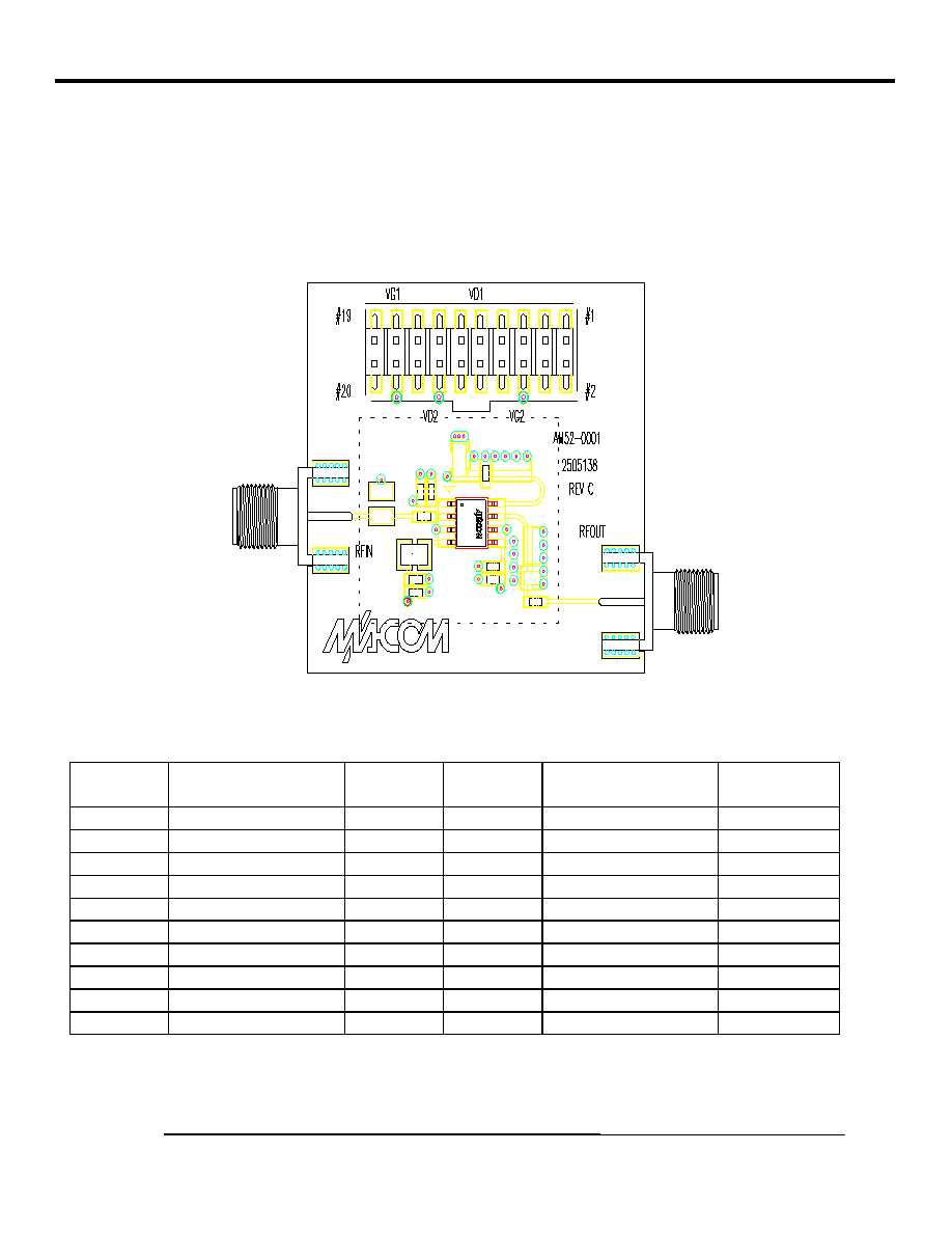
Designer's Kit AM52-0001SMB
The AM52-0001SMB Designer's Kit allows for immediate
evaluation of M/A-COM's AM52-0001. The evaluation board
consists of an AM52-0001, recommended external surface mount
circuitry, RF connectors, and a DC multi-pin connector, all mounted
to a multi-layer FR-4 PCB. Other items included in the Designer's
Kit, a floppy disk (with typical performance data and a DXF file of
the recommended PCB layout) and any additional Application
Notes. The AM52-0001SMB evaluation PCB is illustrated below
with all functional ports labeled.
AMPLIFIER PCB
DC Connector Pinout
PCB DC
Connector
Function
Device Pin
Number
PCB DC
Connector
Function
Device Pin
Number
1
GND
6 & 9 (Puck)
11
2
12
3
13
4
14
VD2
8
5
15
6
VG2
5
16
7
17
VG1
1
8
18
9
VD1
4
19
GND
6 & 9 (Puck)
10
20
1.2 W High Efficiency Power Amplifier
AM52-0001
V1.00
Specifications Subject to Change Without Notice.
6
M/A-COM Inc.
North America: Tel. (800) 366-2266
Asia/Pacific: Tel. +81 3 3226-8761
Europe:
Tel. +44 (1344) 869-595
Fax (800) 618-8883 Fax +81 3 3226-8769
Fax +44 (1344) 300 020
Designer's Kit Biasing Procedure
In order to prevent transients which may damage the MMIC, please adhere to the following procedure.
Turn on all power supplies and set all voltages to 0 volts BEFORE connecting the power supplies to the DC connector.
Apply a -5.0 volt supply to DC connector pin 17 (V
G1
)
Apply a -5.0 volt supply to DC connector pin 6 (V
G2
)
Apply a +5.0 volt supply to the DC connector pin 9 (V
D1
)
Apply a +5.0 volt supply to the DC connector pin 14 (V
D2
)
Adjust all V
GG
supplies to -5 volts
Adjust all V
DD
supplies to +4.8 volts
Adjust V
GG
= V
G1
= V
G2
supply for desired V
DD
quiescent current (typically 150 mA)
To power off, reverse above procedure
1)
Set V
D1
& V
D2
to 0 volts
2)
Set V
G1
& V
G2
to 0 volts
3)
Disconnect bias lines from DC connector
4)
Turn off power supplies
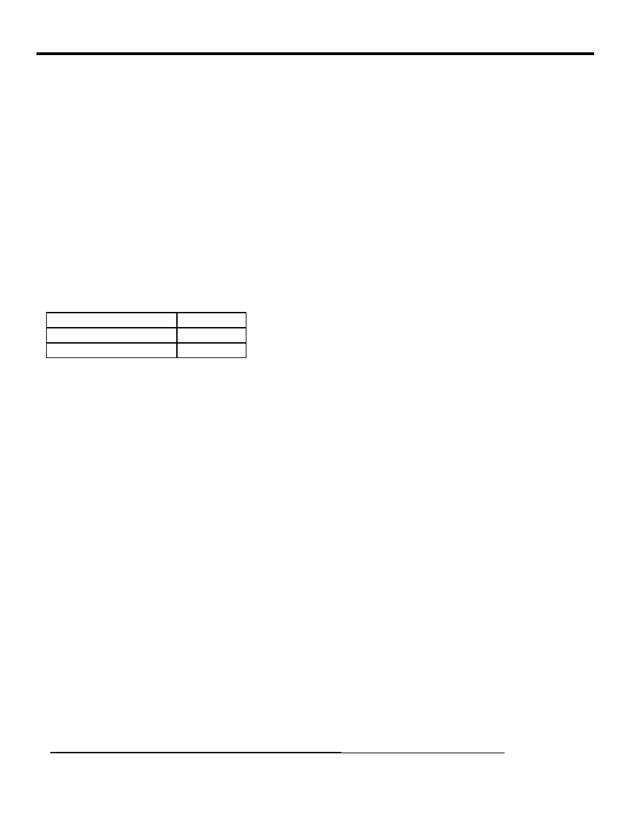
Evaluation PCB + RF Connector Losses
Port Reference
Loss (dB)
PA IN
0.1
PA OUT
0.1
The DC connector on the Designer's Kit PCB allows convenient DC line access. This is accomplished by one or more of the
following methods:
1. A mating female multi-pin connector (Newark Electronics Stock # 46F-4658, not included)
2. Wires soldered to the necessary pins (not included)
3. Clip leads (not included)
4. A combination of clip leads or wires and jumpers (jumpers included as required).