Specifications subject to change without notice.
n
North America: Tel. (800) 366-2266
n
Asia/Pacific: Tel.+81-44-844-8296, Fax +81-44-844-8298
n
Europe: Tel. +44 (1344) 869 595, Fax+44 (1344) 300 020
1
Visit www.macom.com for additional data sheets and product information.
Power Amplifier with T/R Switch
for 802.11b
Preliminary Release
V 1.3
Features
�
WLAN and Bluetooth Applications
�
Meets 802.11b Spectral Mask Requirements at +20
dBm PA Output Power
�
Integrated SPDT Switch
�
Integrated Detector
�
Downset Leadframe for Excellent Heat Dissipation
�
High Power, Low Power, Shutdown Modes
Description
The AM52-0023 is a two stage power amplifier designed
for 802.11b and other 2.4 GHz applications. This
product includes a detector and a T/R switch. Transmit
specifications are given at the antenna port and include
the switch insertion loss. The small size and height of
the AM52-0023 make it ideal for PC card applications.
The AM52-0023 has three operating modes; High
Power, Low Power, and Shutdown. The High Power
Mode has both the first and second PA stages biased on
and is achieved by setting both Vctrl1 and Vctrl2 to +3
volts. The Low Power Mode has the first PA stage on
and the second PA stage off and is achieved by setting
Vctrl1 to +3 volts and Vctrl2 to 0 volts. The Shutdown
Mode is achieved by setting both Vctrl1 and Vctrl2 to 0
volts.
Handling Procedures
Please observe the following precautions to avoid
damage to the AM52-0023:
Static Sensitivity
Gallium arsenide integrated circuits are ESD
sensitive and can be damaged by static electricity.
Use proper ESD precautions when handling these
devices.
Ordering Information
Part Number
Description
AM52-0023TR
7 inch, 1000 piece reel
AM52-0023TR-3000
13 inch, 3000 piece reel
AM52-0023SMB
AM52-0023 Sample Test Board
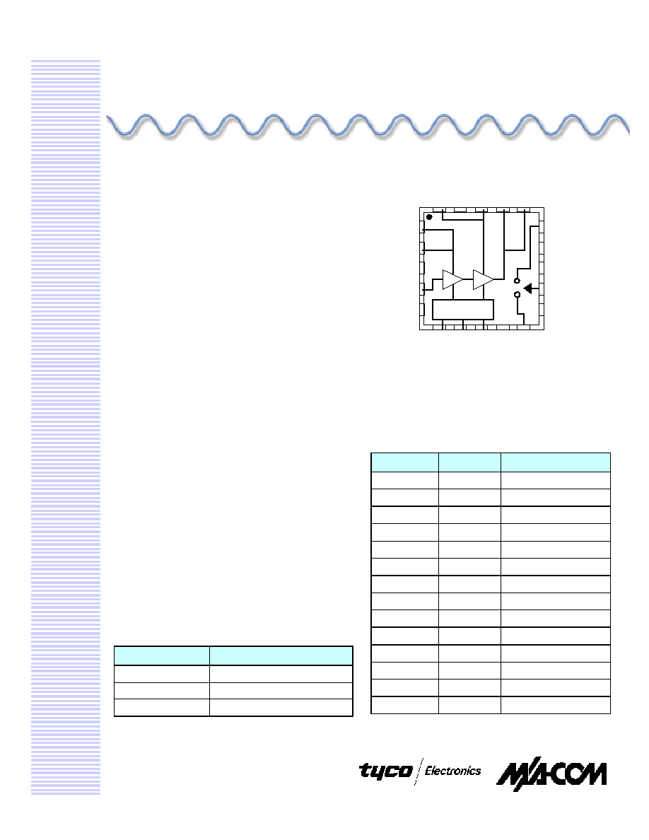
Functional Schematic
1
20
PA
OUT
/
V
SUP
V
SUP
V
CTRL2
NC
RX
SW
TX
NC
TX
SW
RX
ANT
V
SUP
V
DET
V
SUP
V
CTRL
V
SUP
V
SUP
NC
RF
IN
NC
V
CTRL1
Pin Configuration
Pin No.
Function
Description
3, 5, 9, 14
NC
No Connection
4
RF
IN
RF Input to Amplifier
1, 2, 7, 18, 20
V
SUPPLY
DC Supply
6
V
CTRL1
Power Control, Stage 1
8
V
CTRL2
Power Control, Stage 2
10
RX
Receive Port on Switch
11
SW
TX
Switch Control
12
ANT
Switch Antenna Port
13
SW
RX
Switch Control
15
TX
Switch Transmit Port
16
PA
OUT
/V
SUP
PA Output, DC Supply
17
V
DET
Detected Output Power
19
V
CTL
Detector Control
Base
GND
RF/DC Ground
AM52
-
0023
Part Description
Specifications subject to change without notice.
n
North America: Tel. (800) 366-2266
n
Asia/Pacific: Tel.+81-44-844-8296, Fax +81-44-844-8298
n
Europe: Tel. +44 (1344) 869 595, Fax+44 (1344) 300 020
2
Power Amplifier with T/R Switch for 802.11b
AM52-0023
V 1.3
Absolute Maximum Ratings
1
Parameter
Maximum
Max Input Power (2.4 -2.5 GHz)
+ 10 dBm
Operating Voltages
+5.5 volts
Operating Temperature
-40 �C to +85 �C
Channel Temperature
+150 �C
Storage Temperature
-40 �C to +150 �C
1. Exceeding any one or combination of these limits may cause permanent damage.
Electrical Specifications
1,2
: T
C
=+38�C
Parameter
Test Conditions
Units
Min.
Typ.
Max.
Frequency
GHz
2.4
2.5
Control voltage range
V
0.0
3.0
Input Return Loss at RFin
Pin=0 dBm, V
CTRL1
=3.0V, V
CTRL2
=3.0V
Pin=0 dBm, V
CTRL1
=3.0V, V
CTRL2
=0.0V
dB
dB
14
14
24
20
Output Power at ANT
Pin=0 dBm, V
CTRL1
=3.0V, V
CTRL2
=3.0V
Pin=0 dBm, V
CTRL1
=3.0V, V
CTRL2
=0.0V
dBm
dBm
20
0
1 dB Compresson at ANT
V
CTRL1
=3.0V, V
CTRL2
=3.0V
dBm
23
Saturated Power at ANT
V
CTRL1
=3.0V, V
CTRL2
=3.0V
dBm
24
Power Gain at ANT
Pin=0 dBm, V
CTRL1
=3.0V, V
CTRL2
=3.0V
Pin=0 dBm, V
CTRL1
=3.0V, V
CTRL2
=0.0V
dB
dB
18
-2
20
0
Current, Operating
Pin=0 dBm, V
CTRL1
=3.0V, V
CTRL2
=3.0V (High Power Mode)
Pin=0 dBm, V
CTRL1
=3.0V, V
CTRL2
=0.0V (Low Power Mode)
Pin=0 dBm, V
CTRL1
=0.0V, V
CTRL2
=0.0V (Shutdown Mode)
mA
mA
uA
250
22
10
300
30
Control current
Pin=0 dBm, V
CTRL1
=3.0V, V
CTRL2
=3.0V
Pin=0 dBm, V
CTRL1
=3.0V, V
CTRL2
=0.0V
mA
mA
5
0.2
Isolation, Forward (RF
IN
to ANT)
V
CTRL1
=3.0V, V
CTRL2
=0.0V, V
TX
=0.0V, V
RX
=3.0V
dB
45
Isolation, ANT to RX
V
TX
=3.0V, V
RX
=0.0V
dB
18
20
Insertion loss, ANT to RX
V
TX
=0.0V, V
RX
=3.0V
dB
0.7
0.9
Harmonics, all
P
IN
=0 dBm, P
OUT
=23 dBm, V
CTRL1
=3.0V, V
CTRL2
=3.0V
dBc
-40
Detector Output
Pin=0 dBm, V
CTRL1
=3.0V, V
CTRL2
=3.0V
V
1.4
1.6
Duty cycle
%
100
Output Power for Linear Operation
At ANT, Compliance with 802.11b DSSS
dBm
20
Stability
+3.0V<V
CC
<+3.6V, P
OUT
<20dBm, VSWR<6:1,
-25�C< T
C
<+85�C, RBW=3MHz max hold
All spurs <-70dBc
Ruggedness
+3.0V<V
CC
<+5.5V, P
OUT
<23dBm, VSWR<10:1
No permanent damage
1. Test frequency is 2450 MHz unless otherwise specified.
2. Supply voltage is +3.0 volts unless otherwise specificied.
Switch Logic Table
1,2,3
Insertion Loss Path
Isolated Path
SW
RX
SW
TX
RX/ANT
TX/ANT
1
0
TX/ANT
RX/ANT
0
1
1. "0" = 0 +/- 0.2 volts
2. "1" = +2.7 to +5 volts
3. DC Blocking capacitors required on all T/R switch RF ports (pins 10, 12, and 15)
Part Description
Specifications subject to change without notice.
n
North America: Tel. (800) 366-2266
n
Asia/Pacific: Tel.+81-44-844-8296, Fax +81-44-844-8298
n
Europe: Tel. +44 (1344) 869 595, Fax+44 (1344) 300 020
3
Power Amplifier with T/R Switch for 802.11b
AM52-0023
V 1.3
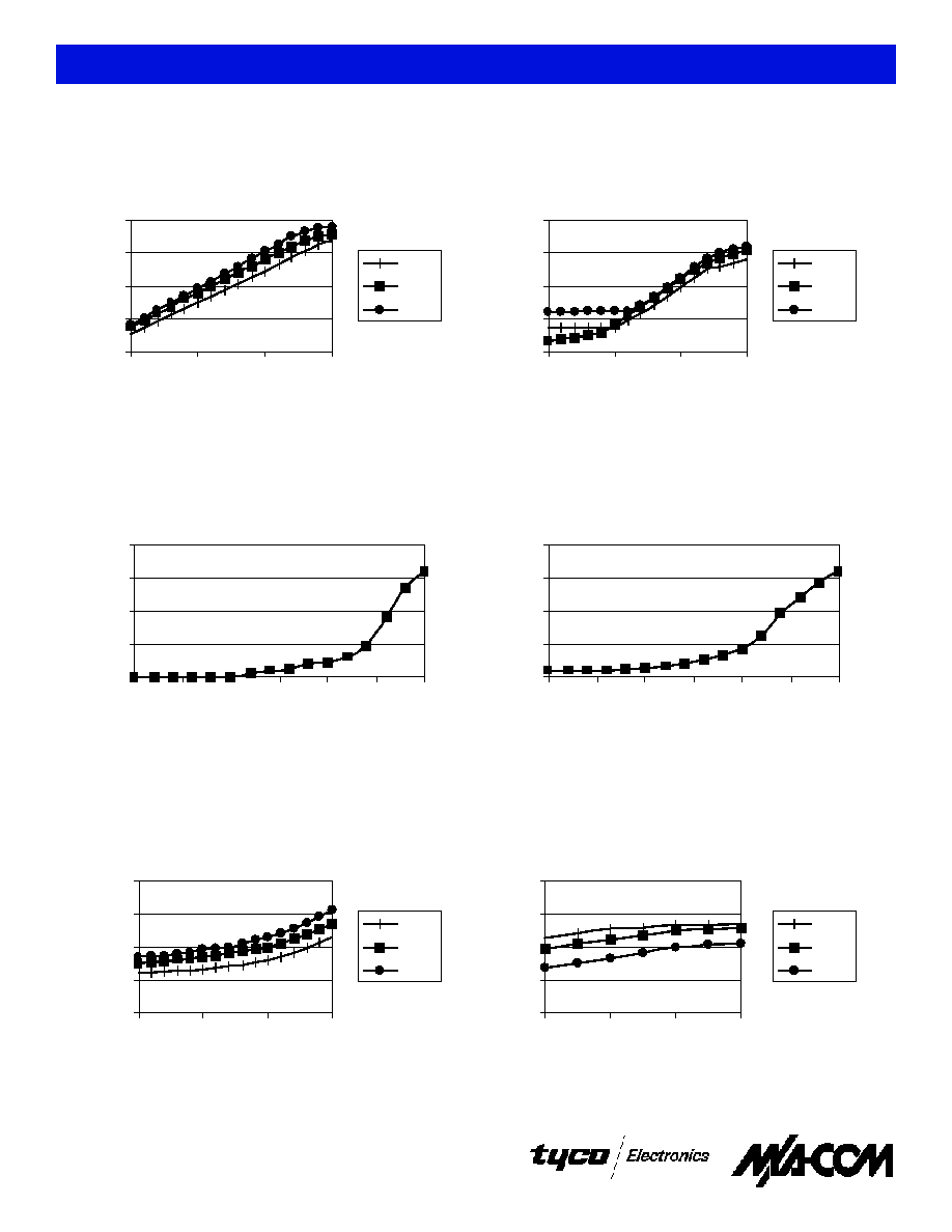
Typical Performance Curves
Output Power, High Power Mode
5
10
15
20
25
-10
-5
0
5
Input Power (dBm)
Output Power (dBm)
+85C
+38C
-40C
Detector Output, High Power Mode
0.5
1
1.5
2
2.5
-10
-5
0
5
Input Power (dBm)
Detector Output (V)
+85C
+38C
-40C
Supply Current, High Power Mode
150
200
250
300
350
-10
-5
0
5
Input Power (dBm)
Supply Current (mA)
+85C
+38C
-40C
Supply Current, Low Power Mode
10
15
20
25
30
2300
2400
2500
2600
Frequency (MHz)
Supply Current (mA)
+85C
+38C
-40C
Detector Output, High Power Mode
0.0
0.5
1.0
1.5
2.0
0.0
0.5
1.0
1.5
2.0
2.5
3.0
Control Voltages 1 and 2 (V)
Detector Output (V)
Detector Output, Low Power Mode
0.0
0.5
1.0
1.5
2.0
0.0
0.5
1.0
1.5
2.0
2.5
3.0
Control Voltage 2 (V)
Detector Output (V)
Part Description
Specifications subject to change without notice.
n
North America: Tel. (800) 366-2266
n
Asia/Pacific: Tel.+81-44-844-8296, Fax +81-44-844-8298
n
Europe: Tel. +44 (1344) 869 595, Fax+44 (1344) 300 020
4
Power Amplifier with T/R Switch for 802.11b
AM52-0023
V 1.3
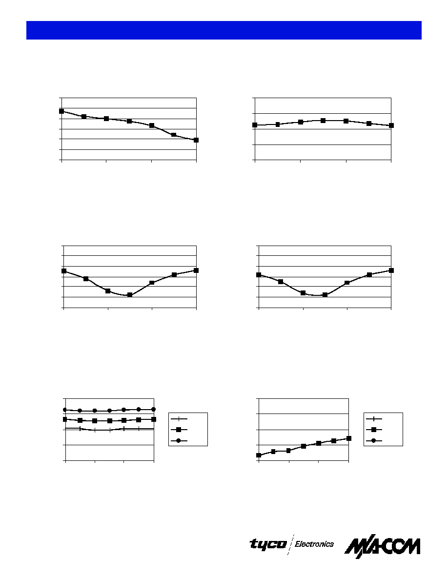
Gain, High Power Mode
16
17
18
19
20
21
22
2300
2400
2500
2600
Frequency (MHz)
Gain (dB)
Gain, Low Power Mode
-2
-1
0
1
2
2300
2400
2500
2600
Frequency (MHz)
Gain (dB)
Input Return Loss, High Power Mode
-30
-25
-20
-15
-10
-5
0
2300
2400
2500
2600
Frequency (MHz)
Return Loss (dB)
Input Return Loss, Low Power Mode
-30
-25
-20
-15
-10
-5
0
2300
2400
2500
2600
Frequency (MHz)
Return Loss (dB)
Switch Insertion Loss
-2
-1.5
-1
-0.5
0
2300
2400
2500
2600
Frequency (MHz)
Insertion Loss (dB)
+85C
+38C
-40C
Switch Isolation
-25
-20
-15
-10
-5
2300
2400
2500
2600
Frequency (MHz)
Isolation (dB)
+85C
+38C
-40C
Part Description
Specifications subject to change without notice.
n
North America: Tel. (800) 366-2266
n
Asia/Pacific: Tel.+81-44-844-8296, Fax +81-44-844-8298
n
Europe: Tel. +44 (1344) 869 595, Fax+44 (1344) 300 020
5
Power Amplifier with T/R Switch for 802.11b
AM52-0023
V 1.3
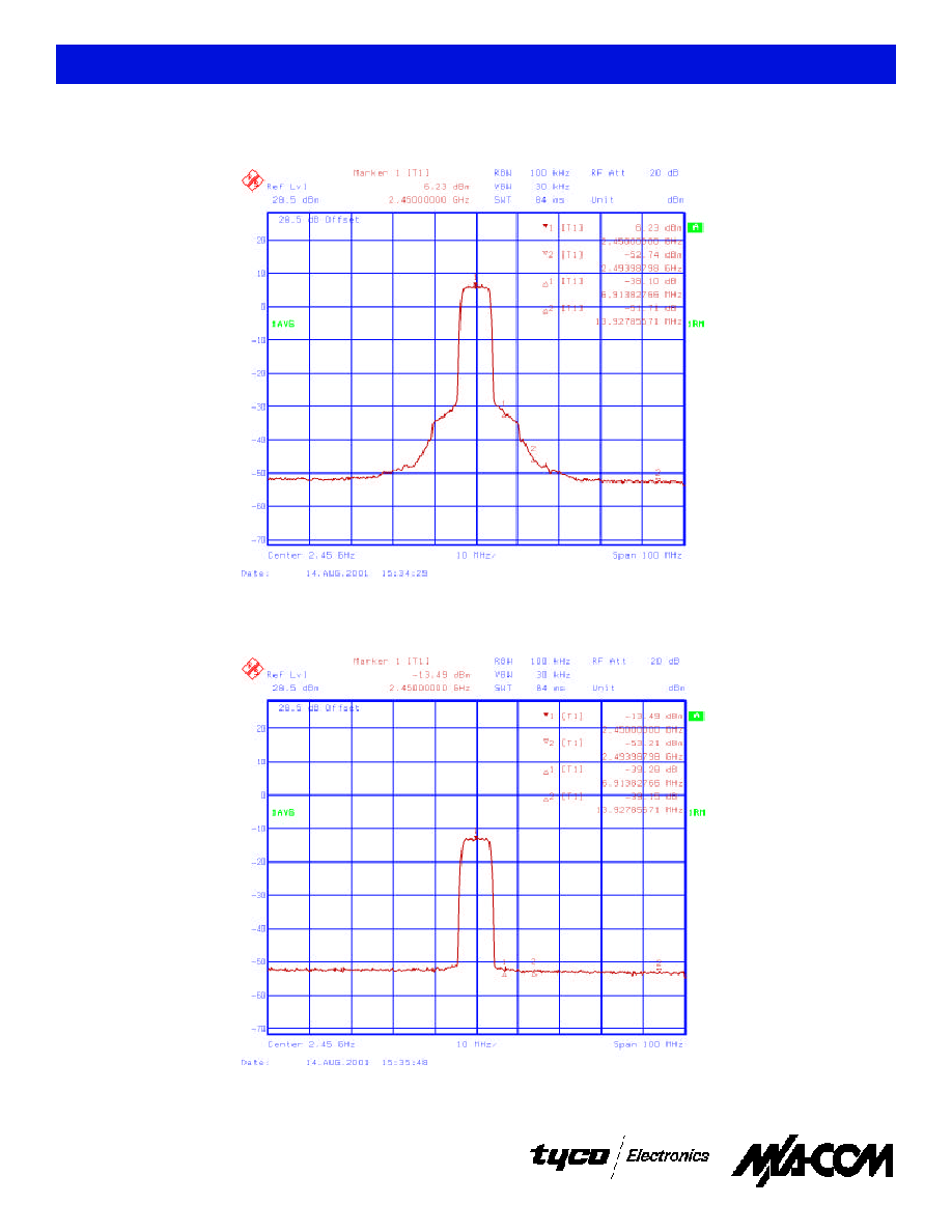
Transmit Spectrum Mask, High Power Mode
Pin = 0 dBm
Transmit Spectrum Mask, Low Power Mode
Pin = 0 dBm
Part Description
Specifications subject to change without notice.
n
North America: Tel. (800) 366-2266
n
Asia/Pacific: Tel.+81-44-844-8296, Fax +81-44-844-8298
n
Europe: Tel. +44 (1344) 869 595, Fax+44 (1344) 300 020
6
Power Amplifier with T/R Switch for 802.11b
AM52-0023
V 1.3
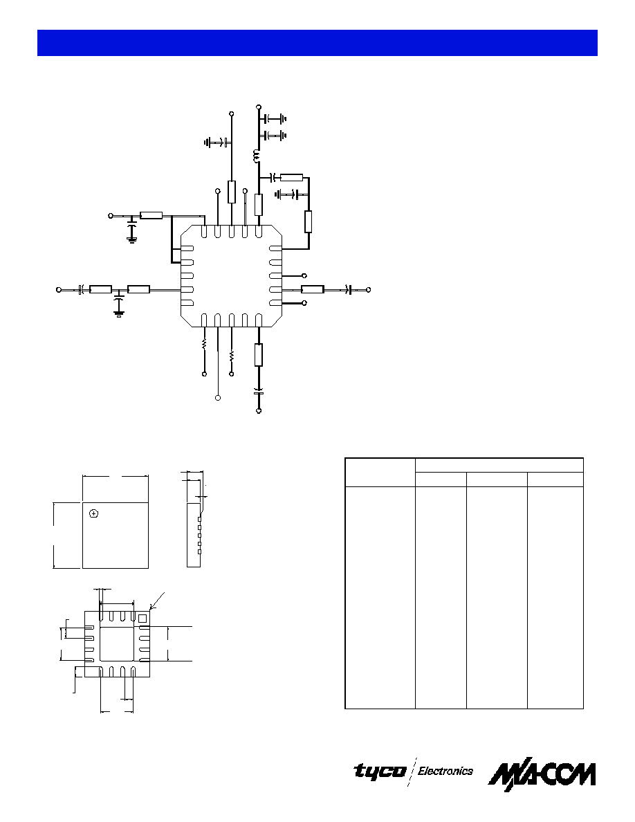
Application Schematic
RFin
Vsup
ANT
Vsup
RXout
Vdet
_out
SW_TX
Vctrl2
TXin
PAout
1pF
0603
Dielectric Labs
2pF
(0603
Dielectric Labs)
33pF (0402 Murata)
6pF (0402 Murata)
22nH
SW_RX
Vsup
Vctrl
AM52-0023
460
2.15k
100pF
Vsup
0.01uF
260mil
140mil
50mil
250mil
1
1 6
6
1 1
PIN:
5. NO CONNECTION
6. PA STAGE 1 CONTROL (+3V/0V)
7. PA STAGE 1 CONTROL SUPPLY (+3V)
10. RF OUT FROM ANT
11. T/R SWITCH CONTROL (+3V/0V)
12. ANT
15. TX IN FROM PA
16. PA OUT, STAGE 2 OUTPUT BIAS (+3V)
20. PA STAGE 1 OUTPUT BIAS (+3V)
19. DETECTOR ON/OFF (+3V/0V)
18. DETECTOR SUPPLY (+3V)
17. DETECTOR OUTPUT
8. PA STAGE 2 CONTROL (+3V/0V) )
13. T/R SWITCH CONTROL (+3V/0V)
14. NO CONNECTION
9. NO CONNECTION
4. RFIN TO PA
3. NO CONNECTION
1. PA STAGE 1 OUTPUT BIAS (+3V)
2. PA STAGE 1 OUTPUT BIAS (+3V)
Cac
200mil
10pF
5 0
5 0
5 0
5 0
50
50
50
2 2
50
ALL TLINE
IMPEDANCES IN
ACCORDANCE WITH 5
MIL-THICK FR-4
4pF (0402 Murata)
60mil
15pF
(0603
Dielectric Labs)
Vctrl1
4 mm, 20 Pin FQFP-N Package
E2
16 x b
e
3 x e
L
e
3 x e
D2
D
E
A
A2
A1
PIN #1
IDENTIFIER
16
1
2
3
4
Measurement (mm)
Dimension
Min.
Nom.
Max.
A
A1
A2
A3
b
D
D1
D2
e
E
E1
E2
L
0.80
0
0
0.23
0.75
0.75
0.50 typ.
0.90
0.02
0.65
0.20 ref.
0.28
4.00 basic
3.75 basic
1.70
0.65 basic
4.00 basic
3.75 basic
1.70
0.60 typ.
1.00
0.05
1.00
0.35
2.25
2.25
0.75 typ.