.025
0,64
.057
±
.003
1,45
±
0,08
.0275
+.0025
-.0025
0,7
+0,06
-0,06
9,91 +0,09
-0,1
.3900
+.0037
-.0041
PIN 1
.236
±
.008
5,99
±
0,2
.004 (0,10)
.007
±
.003
0,18
±
0,08
.010
+.004
-.001
0,25 +0,1
-0,03
.1540
+.0034
-.0043
3,91
+0,09
-0,11
.015 (0,38) X 45
∞
.028
+.022
-.013
0,71
+0,56
-0,33
0-8
∞
.0080
+.0018
-.0005
+0,05
-0,01
0,2
Features
Operates Over Full PCN/PCS/PHS Bands
Operates Over +3 V to +5 V Supply Voltage
+24 dBm P
1dB
Typical at PA Out
35% PAE @ P
1dB
for Linear Operation
On-Chip T/R Switch, Linear Operation to +30 dBm
Low Cost SSOP-28 Plastic Package
Description
M/A-COM's AM55-0004 power amplifier/switch integrates a
power amplifier and transmit/receive switch in a low cost
SSOP package. The power amplifier delivers +24 dBm of
linear power with high efficiency and can be operated at
supply voltages as low as 2.7 V. It is ideally suited for
QPSK or other linearly modulated systems in the 1.8 to 2.0
GHz frequency band.
The power amplifier/switch is fully monolithic and requires
only one output capacitor for power match. The T/R switch
achieves good insertion loss and isolation without degrading
the overall linearity.
The AM55-0004 is ideally suited for final stage power
amplification in linear TDD systems. The integrated switch is
convenient for duplexing. The AM55-0004 can also be used
as a driver stage for high power systems. Typical applications
include Japanese PHS systems or PCN/PCS transmit chains.
M/A-COM's AM55-0004 is fabricated using a mature
0.5-micron gate length GaAs process. The process features
full passivation for increased performance and reliability.
Specifications Subject to Change Without Notice
V2.00
M/A-COM Inc.
s
1011 Pawtucket Boulevard, Lowell, MA 01853 USA
s
Telephone: 800-366-2266
1
250 mW Linear Power Amplifier and T/R Switch
1.8 - 2.0 GHz
AM55-0004
SSOP-28
Preliminary Specifications
Parameter
Units
Min.
Typ.
Max.
Power Amplifier
Linear Gain
dB
22
24
Power Output @ P
1dB
at PA OUT port
dBm
22.5
24
Current From Positive Supply @ P
1dB
mA
75
175
275
Input VSWR
2.0:1
T/R Switch
Insertion Loss
dB
0.6
1.0
Input Match
1.5:1
Isolation
dB
15
20
Typical Electrical Specifications
Test conditions: Frequency: 1.9 GHz, V
DD1
= V
DD2
= 4.8 V ±10%, V
G1
adjusted for 30 mA quiescent bias on V
DD1
,
V
G2
adjusted for 65 mA quiescent bias on V
DD2
, T
A
= +25∞C
q
q
q
q
q
q
Part Number
Description
AM55-0004
SSOP 28-Lead Plastic Package
AM55-0004TR
Forward Tape & Reel
*
AM55-0004RTR
Reverse Tape & Reel
*
AM55-0004SMB
Designer's Kit
Ordering Information
*
If specific reel size is required, consult factory for part
number assignment.
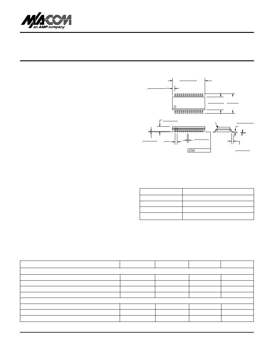
Dimensions are inches over millimeters.
Pin No.
Pin Name
Description
1
GND
DC and RF Ground
2
VSW
Complimentary T/R Switch Control,
-4 V Tx mode/0 V Rx mode
3
GND
DC and RF Ground
4
Tx IN
Transmit side of T/R switch
5
GND
DC and RF Ground
6
GND
DC and RF Ground
7
ANT IN/OUT
Common port of T/R switch which
is connected to the antenna
8
GND
DC and RF Ground
9
Rx OUT
Receive side of T/R switch
10
GND
DC and RF Ground
11
GND
DC and RF Ground
12
V
DD
1
Positive bias for the first stage of
PA, +2.7 to +6.0 volts
13
SAVE Tx
Sleep mode control of first stage of
PA ONLY
0 V -- first PA stage on
-4 V -- first PA stage off
14
GND
DC and RF Ground
15
GND
DC and RF Ground
16
PA IN
RF input of the Power Amplifier
17
GND
DC and RF Ground
18
V
G1
Negative bias control for the first PA
stage, voltage divider is on the MMIC,
adjusted to set V
DD1
quiescent bias
current, which is typically 30 mA.
Input impedance: 10 k
19
GND
DC and RF Ground
20
V
G2
Negative bias control for the second
PA stage, adjusted to set V
DD2
quiescent bias current, which is
typically 65 mA.
Input impedance: > 1M
21
GND
Second Stage DC and RF Ground
22
GND
Second Stage DC and RF Ground
23
GND
Second Stage DC and RF Ground
24
GND
Second Stage DC and RF Ground
25
PA OUT
RF output of the Power Amplifier
26
V
DD2
Positive bias for the second stage of
the PA, +2.7 to +6.0 volts
27
VSW
T/R Switch Control, 0 V Tx mode/-4 V
Rx mode
28
GND
DC and RF Ground
250 mW Linear Power Amplifier and T/R Switch
AM55-0004
Specifications Subject to Change Without Notice
V 2.00
M/A-COM Inc.
s
1011 Pawtucket Boulevard, Lowell, MA 01853 USA
s
Telephone: 800-366-2266
2
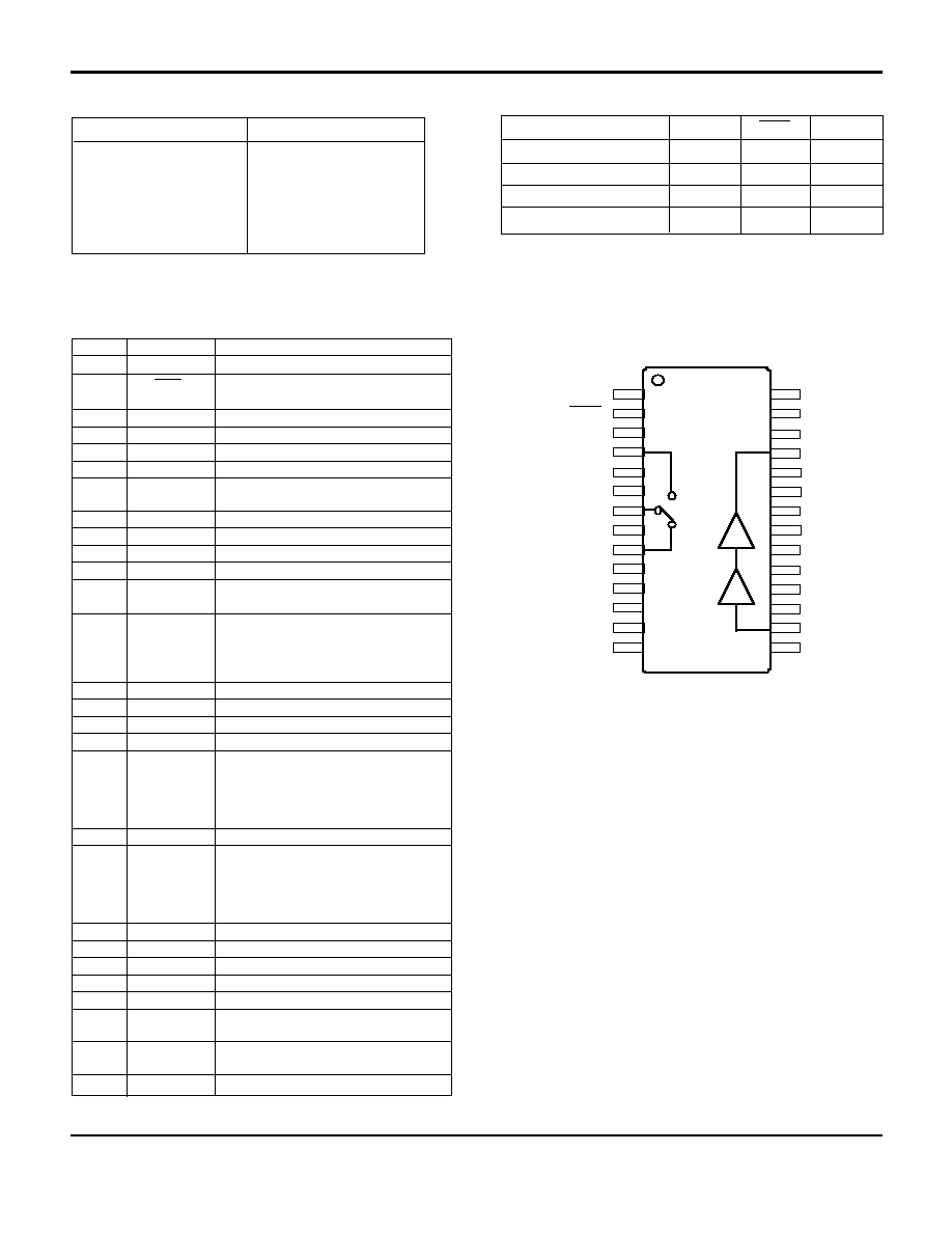
Pin Configuration
Functional Diagram and Pin Configuration
Absolute Maximum Ratings
1
Parameter
Absolute Maximum
Max. Input Power
2
+23 dBm
Operating Voltages
2
V
DD
= 7 V
V
GG
= -5 V
V
DD
- V
GG
= 8 V
Operating Temperature
-40∞C to +85∞C
Storage Temperature
-65∞C to +150∞C
1. Exceeding these limits may cause permanent damage.
2. Ambient temperature (T
A
) = +25∞C
Truth Table
Operating Mode
VSW
VSW
SAVE Tx
PA Tx
X
X
0 V
PA Sleep
X
X
-4.0 Volts
T/R Switch Tx
0 Volts
-4.0 Volts
X
T/R Switch Rx
-4.0 Volts
0 Volts
X
X - Don't Care
1
28
14
15
GND
VSW
GND
GND
VSW
Tx IN
GND
GND
GND
GND
GND
GND
GND
GND
GND
GND
GND
GND
GND
ANT IN/OUT
Rx OUT
V
DD1
V
DD1
V
G1
V
G2
SAVE Tx
PA IN
PA OUT
V
DD2
V
G2
V
G1
250 mW Linear Power Amplifier and T/R Switch
AM55-0004
Specifications Subject to Change Without Notice
V 2.00
M/A-COM Inc.
s
1011 Pawtucket Boulevard, Lowell, MA 01853 USA
s
Telephone: 800-366-2266
3
Power Amplifier Small Signal Performance
1
Power Amplifier CW Performance at 1.9 GHz
1
GAIN
FREQUENCY (GHz)
1.50
1.75
2.00
2.25
2.50
27
24
21
18
15
GAIN (dB)
POWER OUTPUT
P
IN
(dBm)
-5
-3
-1
1
3
28
26
24
22
20
18
POWER (dBm)
INPUT MATCH
FREQUENCY (GHz)
1.50
1.75
2.00
2.25
2.50
0
-5
-10
-15
-20
-25
RETURN LOSS (dB)
POWER ADDED EFFICIENCY (%)
P
IN
(dBm)
-5
-3
-1
1
3
45
35
25
15
5
PAE (%)
OUTPUT MATCH
FREQUENCY (GHz)
1.50
1.75
2.00
2.25
2.50
0
-5
-10
-15
-20
-25
RETURN LOSS (dB)
GAIN COMPRESSION
P
IN
(dBm)
-5
-3
-1
1
3
0
-1
-2
-3
-4
-5
COMPRESSION (dB)
6.0 V
4.8 V
3.6 V
3.0 V
6.0 V
4.8 V
3.6 V
3.0 V
6.0 V
4.8 V
3.6 V
3.0 V
6.0 V
4.8 V
3.6 V
3.0 V
6.0 V
4.8 V
3.6 V
3.0 V
6.0 V
4.8 V
3.6 V
3.0 V
1. All data measured at T
A
= +25∞C and V
G1
, V
G2
adjusted for first stage quiescent current of 30 mA and second stage current of 65 mA,
respectively.
250 mW Linear Power Amplifier and T/R Switch
AM55-0004
Specifications Subject to Change Without Notice
V 2.00
M/A-COM Inc.
s
1011 Pawtucket Boulevard, Lowell, MA 01853 USA
s
Telephone: 800-366-2266
4
Power Amplifier Temperature Performance
1
LINEAR GAIN, V
DD1
= V
DD2
= 4.8 V
FREQUENCY (GHz)
1.50
1.75
2.00
2.25
2.50
27
24
21
18
15
GAIN (dB)
POWER OUTPUT @ 1.9 GHz, V
DD1
= V
DD2
= 4.8 V
P
IN
(dBm)
-5
-3
-1
1
3
28
26
24
22
20
18
POWER (dBm)
POWER ADDED EFFICIENCY (%) @ 1.9 GHz,
V
DD1
= V
DD2
= 4.8 V
P
IN
(dBm)
-5
-3
-1
1
3
40
35
30
25
20
15
10
PAE (%)
-15∞C
+25∞C
+70∞C
-15∞C
+25∞C
-15∞C
+25∞C
+70∞C
Power Amplifier Spurious Response at
Various Supply Voltages
1
THIRD ORDER INTERMODULATION RATIO @ 1.9 GHz
(TONE SPACING 600 KHz)
FUNDAMENTAL P
OUT
/TONE (dBm)
15
17
19
21
23
25
30
25
20
15
10
IMR (dBc)
2ND HARMONIC RATIO @ 1.9 GHz
FUNDAMENTAL P
OUT
(dBm)
10
13
16
19
22
25
60
50
40
30
20
dBc
3RD HARMONIC RATIO @ 1.9 GHz
FUNDAMENTAL P
OUT
(dBm)
10
13
16
19
22
25
80
75
70
65
60
55
50
dBc
6.0 V
4.8 V
3.6 V
3.0 V
4.0 V
4.8 V
3.0 V
4.0 V
4.8 V
3.0 V
1. All data measured at T
A
= +25∞C and V
G1
, V
G2
adjusted for first stage quiescent current of 30 mA and second stage current of 65 mA, respectively.
+70∞C
250 mW Linear Power Amplifier and T/R Switch
AM55-0004
Specifications Subject to Change Without Notice
V 2.00
M/A-COM Inc.
s
1011 Pawtucket Boulevard, Lowell, MA 01853 USA
s
Telephone: 800-366-2266
5
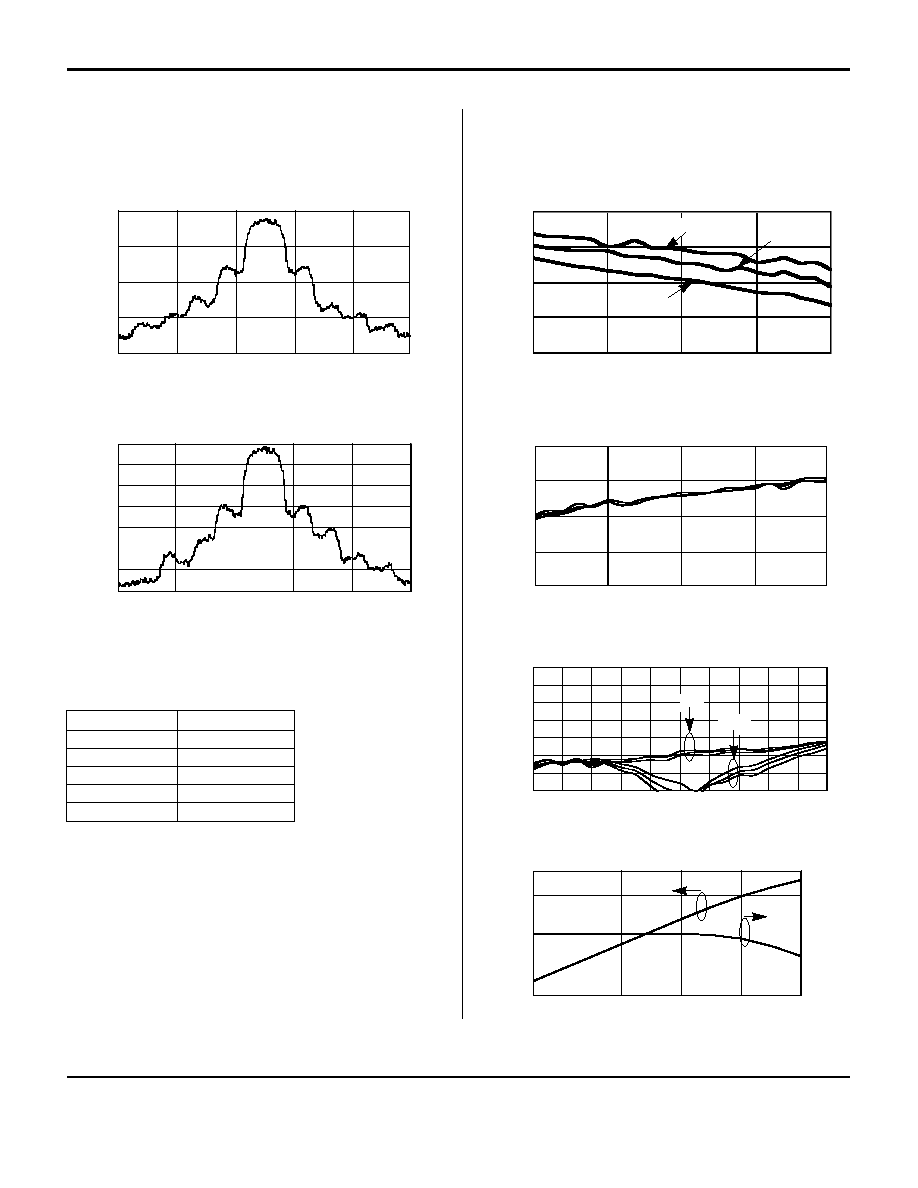
Power Amplifier Spectral Response Under
Modulation Drive
(
/4 DQPSK,
= 0.5, 384 kB/sec, 9-bit PN code)
SPECTRAL RESPONSE UNDER MODULATION
1
(V
D
= 3.0 V, P
OUT
= 20.5 dBm)
FREQUENCY (MHz)
1899.0
1899.4
1899.8
1900.2
1900.6
1901.0
0
-20
-40
-60
-80
POWER SPECTRAL
DENSITY (dBc)
Transmit/Receive Switch Performance
INSERTION LOSS
FREQUENCY (GHz)
1.50
1.75
2.00
2.25
2.50
0.0
-0.5
-1.0
-1.5
-2.0
LOSS (dB)
SPECTRAL RESPONSE UNDER MODULATION
1
(V
D
= 4.8 V, P
OUT
= 23.4 dBm)
FREQUENCY (MHz)
1899.0
1899.4
1899.8
1900.2
1900.6
1901.0
0
-10
-20
-30
-40
-50
-60
-70
POWER SPECTRAL
DENSITY (dBc)
ISOLATION (@ -15∞C, +25∞C and +70∞C)
FREQUENCY (GHz)
1.50
1.75
2.00
2.25
2.50
-20
-25
-30
-35
-40
ISOLATION (dB)
RETURN LOSS (@ -15∞C, +25∞C and +70∞C)
FREQUENCY (GHz)
1.5 1.6
1.7
1.8
1.9
2.0
2.1
2.2
2.3
2.4
2.5
0
-5
-10
-15
-20
-25
-30
-35
RETURN LOSS (dB)
LINEARITY (Tx MODE)
POWER IN (dBm)
25
26
27
28
29
30
31
32
33
34
33
31
29
27
25
23
2.5
1.5
0.5
-0.5
-1.5
-2.5
POWER OUT (dBm)
COMPRESSION
(dB)
V
D
(volts)
P
OUT
(dBm)
3
20.5
3.6
21.4
4
22.2
4.8
23.4
6
23.7
Output Power Under Modulation
2
1. Spectral output is tested under the following conditions:
Modulation scheme is
/4 DQPSK with a bit transfer rate
of 384 kB/sec and a root Nyquist filter with = 0.5 per
RCR STD-28. The spectrum analyzer settings are as follows:
Resolution bandwidth: 10 kHz
Video bandwidth: 100 kHz
Sweep time: 5 seconds
2. This chart documents the modulated output power delivered
for a fixed adjacent channel interference (ACI) rejection of 55
dBc at a 600-kHz offset.
-15∞C
+25∞C
In
Out
+70∞C
External Circuitry
Label
Value
Purpose
C1 - C5
1000 pF
Low frequency bypass
C6 - C8
68 pF
RF bypass
C9
1.5 pF
Output power tuning
C10
15 pF
Reduces low frequency gain
R1
2.7 k
Voltage divider to V
G2
R2
1.5 k
Voltage divider to V
G2
R3
150
Reduces low frequency gain
Tline
0.250 in. long
Power match
250 mW Linear Power Amplifier and T/R Switch
AM55-0004
Specifications Subject to Change Without Notice
V 2.00
M/A-COM Inc.
s
1011 Pawtucket Boulevard, Lowell, MA 01853 USA
s
Telephone: 800-366-2266
6
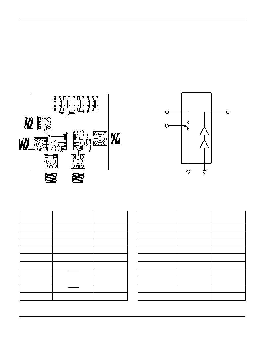
Recommended PCB Configuration
Layout View
Cross-Section View
External Circuitry Parts List
All off-chip components are low-cost surface mount components obtainable from
multiple sources. (0.020 in. x 0.040 in. or 0.030 in. x 0.050 in.)
V
DD1
C8
C5
VSW
Tx IN
Rx OUT
ANT IN/OUT
1
2
3
4
5
6
7
8
9
10
11
12
13
14
28
27
26
25
24
23
22
21
20
19
18
17
16
15
C4
Save Tx
VSW
R2
R1
C1
C6
V
DD2
V
G2
V
G1
C9
PA OUT
C10
C2
PA IN
C3
C7
R3
TLine
The PCB dielectric between RF traces and RF ground layers
should be chosen to reduce RF discontinuities between
50-
lines and package pins. M/A-COM recommends an
FR-4 dielectric thickness of 0.008 in. (0.2 mm), yielding a
50-
line width of 0.015 in. (0.38 mm). The recommended
metalization thickness is 1 oz. copper.
Shaded traces are vias to DC routing layer and traces on DC
routing layer.
Biasing Procedure
The AM55-0004 requires that V
GG
bias be applied prior to
any
V
DD
bias. Permanent damage may occur if this
procedure is not followed. All FETs in the PA will draw
excessive current and damage internal circuitry.
RF Traces + Components
RF Ground
DC Routing
Customer Defined
C1
C6
C9
C2
C10
C7
R2
R1
R3
C3
C4
C5
C8
0.700 in.
0.490 in.
Pin 1
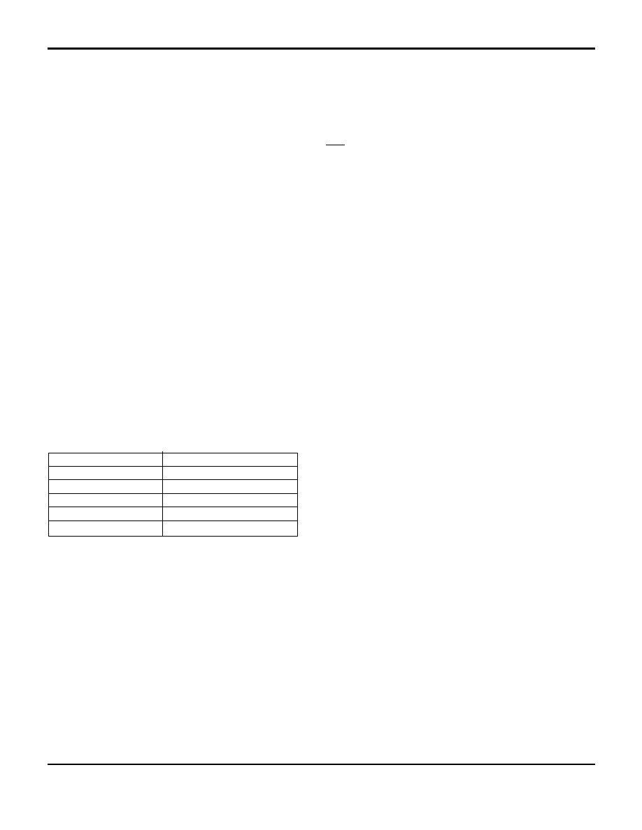
The AM55-0004SMB Designer's Kit allows for immediate evaluation of M/A-COM's AM55-0004 integrated Power Amplifier
and T/R Switch. The evaluation board consists of an AM55-0004, recommended external surface mount circuitry, RF
connectors and a DC multipin connector, all mounted to a multi-layer FR-4 PCB. Other items included in the Designer's Kit:
a floppy disk (with typical performance data and a .DXF file of the recommended PCB layout) and any additional
Application Notes. The AM55-0004SMB PA/Switch evaluation PCB and block diagram are illustrated below with all
functional ports labeled.
PCB DC
Function
Device Pin
PCB DC
Function
Device Pin
Connector
Number
Connector
Number
1
N/C
N/C
11
VSW
27
2
V
DD1
(+ 4.8 V)
12
12
V
G1
18
3
SAVE Tx (0 V/-4 V)
13
13
VSW
27
4
GND
N/C
14
GND
N/C
5
SAVE Tx (0 V/-4 V)
13
15
V
G2
20
6
V
G1
18
16
V
G1
18
7
VSW
2
17
N/C
N/C
8
GND
N/C
18
V
G2
20
9
VSW
2
19
N/C
N/C
10
V
G1
18
20
V
DD2
( + 4.8 V)
26
PA OUT
PA IN
RX OUT
ANT IN/OUT
TX IN
VDD1
SAVE T
VSW
VSW VG2
VG1
VDD2
250 mW Linear Power Amplifier and T/R Switch
AM55-0004
Specifications Subject to Change Without Notice
V 2.00
M/A-COM Inc.
s
1011 Pawtucket Boulevard, Lowell, MA 01853 USA
s
Telephone: 800-366-2266
7
Designer's Kit (AM55-0004SMB)
P/A Switch Sample Board
Functional Block Diagram
Tx IN
ANT IN/OUT
Rx OUT
PA IN
PA OUT
DC Connector Pinout
250 mW Linear Power Amplifier and T/R Switch
AM55-0004
Specifications Subject to Change Without Notice
V 2.00
M/A-COM Inc.
s
1011 Pawtucket Boulevard, Lowell, MA 01853 USA
s
Telephone: 800-366-2266
8
In order to prevent transients which may damage the MMIC, please adhere to the following procedure.
∑ Turn on all power supplies and set all voltages to 0 volts BEFORE connecting the power supplies to the
DC connector.
∑ Apply -4.0 volt supply or GND to DC connector pin 9 (VSW, see truth table for desired mode).
∑ Apply -4.0 volt supply or GND to DC connector pin 13 (VSW, see truth table for desired mode).
∑ Apply a -4.0 volt supply to the DC connector pin 16 (V
G1
).
∑ Apply a -4.0 volt supply to the DC connector pin 18 (V
G2
).
∑ Apply a +4.8 volt supply to the DC connector pin 2 (V
DD1
).
∑ Apply a +4.8 volt supply to the DC connector pin 20 (V
DD2
).
∑ Apply GND to DC connector pin 5 (Save Tx).
∑ Adjust V
G1
supply for desired V
DD1
quiescent current (typically 30 mA).
∑ Adjust V
G2
supply for desired V
DD2
quiescent current (typically 65 mA).
∑ Change voltage on DC connector pin 5 as required (Save Tx, see truth table for desired mode).
∑ Apply RF power and test.
∑ To power off, reverse above procedure
1. Set V
G1
& V
G2
to -4 V.
2. Set V
DD1
& V
DD2
to 0 V.
3. Set control voltage supplies to 0 V.
4. Disconnect bias lines from DC connector.
5. Turn off power supplies.
Port Reference
Estimated Loss (dB)
PA IN
0.15
PA OUT
0.20
Tx IN
0.20
ANT IN/OUT
0.20
Rx OUT
0.20
AM55-0004SMB Biasing Procedure
Evaluation PCB and RF Connector Losses
The DC connector on the Designer's Kit PCB allows selection of all the device's operating modes.
It is accomplished by one or more of the following methods:
1. A mating female multi-pin connector (Newark Electronics
Stock # 46F-4658, not included)
2. Wires soldered to the necessary pins (not included)
3. Clip leads (not included)
4. A combination of clip leads or wires and jumpers
(jumpers included as required)