V2.00
Switched Low Noise Amplifier, 800-1000 MHz
AM55-0016
M/A-COM Division of AMP Incorporated
s
North America: Tel. (800) 366-2266, Fax (800) 618-8883
s
Asia/Pacific: Tel.+85 2 2111 8088, Fax +85 2 2111 8087
s
Europe: Tel. +44 (1344) 869 595, Fax+44 (1344) 300 020
www.macom.com
AMP and Connecting at a Higher Level are trademarks.
Specifications subject to change without notice.
* If specific reel size is required, consult factory for part number.
Ordering Information
Part Number
Package
AM55-0016
MSOP 8-Lead Plastic Package
AM55-0016TR
Forward Tape and Reel*
AM55-0016RTR
Reverse Tape and Reel*
AM55-0016SMB
Designer's Kit
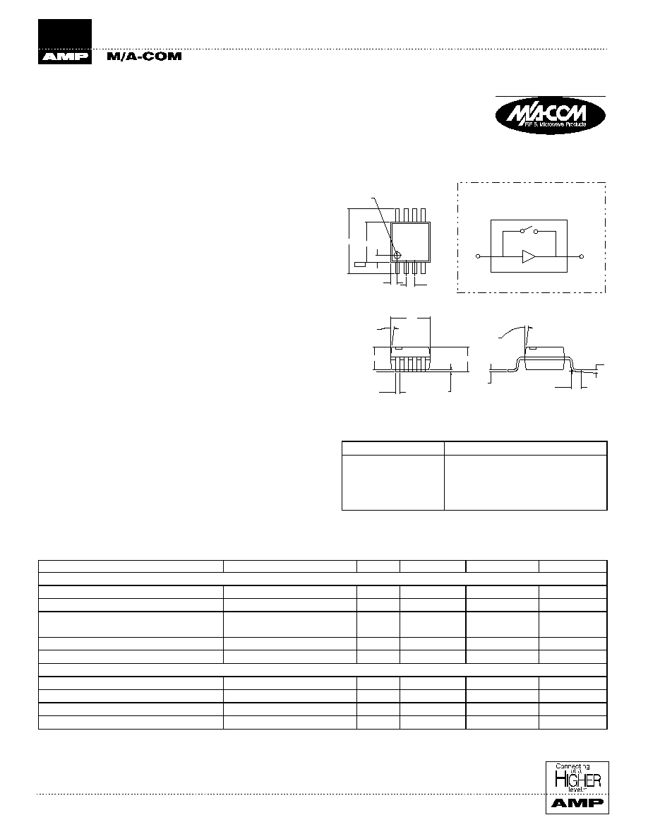
MSOP-8
Features
�
High Gain State:
- Gain: 16dB, Noise Figure: 1.6dB
- Input IP3: +3dBm (@2.7V, 25mA)
�
Low Gain State:
- Insertion Loss: 5dB, Input IP3: +24dBm
�
Single Supply: +2.7 to +5 VDC
�
Low Cost MSOP-8 Plastic Package
�
Adjustable current: 10 to 30 mA with external resistor
Description
M/A-COM's AM55-0016 is a high dynamic range, switchable
low noise amplifier in a low cost, MSOP 8-lead, surface mount,
plastic package. The design utilizes a patented switching
technique to provide a low insertion loss, high input IP
3
bypass
state in parallel with the high gain, low noise state. The LNA
employs external input matching to obtain optimum noise figure
performance and operating frequency flexibility. The
AM55-0016 also features flexible biasing to control the current
consumption vs. dynamic range trade-off. Its current can be
controlled over a range of 10 mA to 30 mA with an external
resistor.
Typical applications include receiver front ends in cellular band
CDMA handsets. It is also useful as a switched gain block, buffer
or driver in portable cellular systems.
The AM55-0016 is fabricated using a low-cost 0.5-micron gate
length GaAs MESFET process. The process features full
passivation for increased performance and reliability.
Switched Low Noise Amplifier
800 - 1000 MHz
AM55-0016
-B-
ID PIN
0.193
010
R
0 118
.020
020
0.0256
0 118
12�
4X
0 034
0 040
0 008
0 013
12�
4X
0.007
0 0215
3�
RF
IN
RF
OUT
Functional Block Diagram
Electrical Specifications
1
T
A
= +25�C, Z
0
=50
, F=881 MHz, P
IN
= -30 dBm, V
DD
=2.7 V, I
DD
=10 mA
Parameter
Test Conditions
Units
Min.
Typ.
Max.
HIGH GAIN STATE, Voltage control = 2.7 volts
Gain
dB
--
16
--
Noise Figure
dB
--
1.6
1.8
Input IP3
I
DD
= 10 mA, V
DD
= 2.7V
I
DD
= 25 mA, V
DD
= 2.7V
dBm
dBm
--
--
-2
+3
--
--
Input VSWR / Output VSWR
--
--
2.0:1
Reverse Isolation
dB
--
32
--
LOW GAIN STATE, Voltage control = 0 volts
Insertion Loss
I
DD
= 100
�
A
dB
--
5
--
Input IP3
dBm
--
+24
--
Input VSWR
--
--
2.3:1
--
Output VSWR
--
--
2.0:1
--
1. Refer to
Typical Performance Data for performance versus frequency and bias.
V2.00
Switched Low Noise Amplifier, 800-1000 MHz
AM55-0016
M/A-COM Division of AMP Incorporated
s
North America: Tel. (800) 366-2266, Fax (800) 618-8883
s
Asia/Pacific: Tel.+85 2 2111 8088, Fax +85 2 2111 8087
s
Europe: Tel. +44 (1344) 869 595, Fax+44 (1344) 300 020
www.macom.com
AMP and Connecting at a Higher Level are trademarks.
Specifications subject to change without notice.
L1
RFOUT
RFIN
VDD
VCTL
RBIAS
C1
C2
C6
C4
C3
C5
C7
U1
1
2
3
4
5
6
7
8
RF Traces + Components
RF Ground
DC Routing
Customer Defined
The PCB dielectric between RF traces and RF ground layers
should be chosen to reduce RF discontinuities between 50
lines and package pins. M/A-COM recommends an FR-4
dielectric thickness of 0.008" (0.2 mm) yielding a 50
line
width of 0.015" (0.38 mm). The recommended metalization
thickness is 1 ounce copper.
U2
C2
C4
C6
C7
C5
C3
L1
C1
U1
RBIAS
External Circuitry Parts List
1
Part
Value
Purpose
C1, C2
1000 pF
Source Bypass
C3, C4
47 pF
By-Pass
C5, C6, C7
10 nF
By-Pass
L1
22 nH
Tuning
RBIAS
see note 2
Source Bias Resistor
U1
UMH9N
Dual Bipolar Transistor
1. All external circuitry parts are readily available, low cost surface
mount components (0.040 inches x 0.020 inches or 0.060 inches x
0.030 inches).
2. RBIAS is chosen to set the desired current,
For:
I
dd
~10 mA, R1 = 75 ohms;
I
dd
~20 mA, R1 = 25 ohms;
I
dd
~30 mA, R1 = 9 ohms.
Layout View
Absolute Maximum Ratings
1
Parameter
Absolute Maximum
V
DD
+6 VDC
Input Power
0 dBm
Current
30 mA
Channel Temperature
2
+150�C
Operating Temperature
-40�C to +85�C
Storage Temperature
-65�C to +150�C
1. Exceeding any one or combination of these limits may cause
permanent damage.
2. Typical thermal resistance (
jc
) = +99�C/W.
Pin Configuration
External Circuitry
Cross Section View
Recommended PCB Configuration
Pin No.
Pin Name
Description
1
VDD1
Stage 1 Supply Voltage
2
IN
RF Input
3
VS1
Stage 1 Source
4
GND
RF and DC Ground
5
VS2
Stage 2 Source
6
OUT
RF Output
7
VDD2
Stage 2 Supply Voltage
8
VCTL
Switch Control Voltage
V2.00
Switched Low Noise Amplifier, 800-1000 MHz
AM55-0016
M/A-COM Division of AMP Incorporated
s
North America: Tel. (800) 366-2266, Fax (800) 618-8883
s
Asia/Pacific: Tel.+85 2 2111 8088, Fax +85 2 2111 8087
s
Europe: Tel. +44 (1344) 869 595, Fax+44 (1344) 300 020
www.macom.com
AMP and Connecting at a Higher Level are trademarks.
Specifications subject to change without notice.
12
13
14
15
16
17
18
19
800
850
900
950
1000
Frequency (MHz)
Gain (dB)
10mA
20mA
30mA
1.0
1.1
1.2
1.3
1.4
1.5
1.6
1.7
1.8
1.9
2.0
800
850
900
950
1000
Frequency (MHz)
Noise Figure (dB)
10mA
20mA
30mA
Typical Performance Data
Test Conditions: T
A
= +25�C, Z
0
= 50
, V
DD
= 2.7V, I
DD
= 10mA unless otherwise specified.
-3
-2
-1
0
1
2
3
4
5
6
7
800
850
900
950
1000
Frequency (MHz)
IIP3 (dBm)
10mA
15mA
20mA
25mA
-2
0
2
4
6
8
10
10
12
14
16
18
20
22
24
26
28
30
Current (mA)
IIP3 (dBm)
2.7V
3.2V
3.6V
4.0V
-7.0
-6.5
-6.0
-5.5
-5.0
-4.5
-4.0
-3.5
-3.0
-2.5
-2.0
800
850
900
950
1000
Frequency (MHz)
Insertion Loss (dB)
20
21
22
23
24
25
26
27
28
29
30
IIP3 (dBm)
10
11
12
13
14
15
16
17
18
-26
-24
-22
-20
-18
-16
-14
-12
-10
Input Power (dBm)
Gain (dB)
-10
-8
-6
-4
-2
0
2
4
6
Output Power (dBm)
HIGH GAIN MODE: Input IP3 vs. Current
HIGH GAIN MODE: IIP3 vs. Current and Voltage
LOW GAIN MODE:
Insertion Loss and Input IP3
HIGH GAIN MODE:
Gain and Output Power vs. Input Power
HIGH GAIN MODE: Gain versus Current
HIGH GAIN MODE: Noise Figure versus Current
-20
-18
-16
-14
-12
-10
-8
-6
-4
-2
0
800
850
900
950
1000
Frequency (MHz)
Return Loss (dB)
Low Gain
High Gain
-20
-18
-16
-14
-12
-10
-8
-6
-4
-2
0
800
850
900
950
1000
Frequency (MHz)
Return Loss (dB)
INPUT RETURN LOSS
OUTPUT RETURN LOSS
Low Gain
High Gain
V2.00
Switched Low Noise Amplifier, 800-1000 MHz
AM55-0016
M/A-COM Division of AMP Incorporated
s
North America: Tel. (800) 366-2266, Fax (800) 618-8883
s
Asia/Pacific: Tel.+85 2 2111 8088, Fax +85 2 2111 8087
s
Europe: Tel. +44 (1344) 869 595, Fax+44 (1344) 300 020
www.macom.com
AMP and Connecting at a Higher Level are trademarks.
Specifications subject to change without notice.
Typical Performance Data (continued)
12
13
14
15
16
17
18
19
800
850
900
950
1000
Frequency (MHz)
Gain (dB)
-30C
+25C
+80C
1.0
1.2
1.4
1.6
1.8
2.0
2.2
2.4
800
850
900
950
1000
Frequency (MHz)
Noise Figure (dB)
-30C
+25C
+80C
-6.0
-5.8
-5.6
-5.4
-5.2
-5.0
-4.8
-4.6
-4.4
-4.2
-4.0
800
850
900
950
1000
Frequency (MHz)
Insertion Loss (dB)
-30C
+25C
+80C
HIGH GAIN MODE: Gain vs. Temperature
HIGH GAIN MODE: Noise Figure vs. Temperature
LOW GAIN MODE: Insertion Loss vs. Temperature
The AM55-0016SMB Designer's Kit allows for immediate evaluation of M/A-COM's AM55-0016. The Designer's Kit includes an
AM55-0016, an evaluation board and a floppy disk containing typical performance data and a DXF file of the recommended PCB layout.
The evaluation board consists of the recommended external surface mount circuitry, RF connectors and a DC multi-pin connector, all
mounted to a multi-layer FR-4 PCB. The AM55-0016SMB evaluation PCB is illustrated below with all functional ports labeled.
Designer's Kit AM55-0016SMB
AM55-0016 Evaluation Board
Evaluation PCB + RF Connector Losses
Port Reference
Approximate RF Loss
RF IN
0.15 dB @ 900 MHz
RF OUT
0.15 dB @ 900 MHz
The DC connector on the Designer's Kit PCB allows convenient
DC line access. This is accomplished by one or more of the
following methods:
1. A mating female multi-pin connector
(Newark Electronics Stock # 46F-4658, not included).
2. Wires soldered to the necessary pins (not included).
3. Clip leads (not included).
9
RF OUT
AV10367
REV -
GND
RF IN
10
2
1
4
3
6
5
8
7