n
North America: Tel. (800) 366-2266, Fax (800) 618-8883
n
Asia/Pacific: Tel.+81-44-844-8296, Fax +81-44-844-8298
n
Europe: Tel. +44 (1344) 869 595, Fax+44 (1344) 300 020
Specifications subject to change without notice.
Visit www.macom.com for additional data sheets and product information.
V 2.0
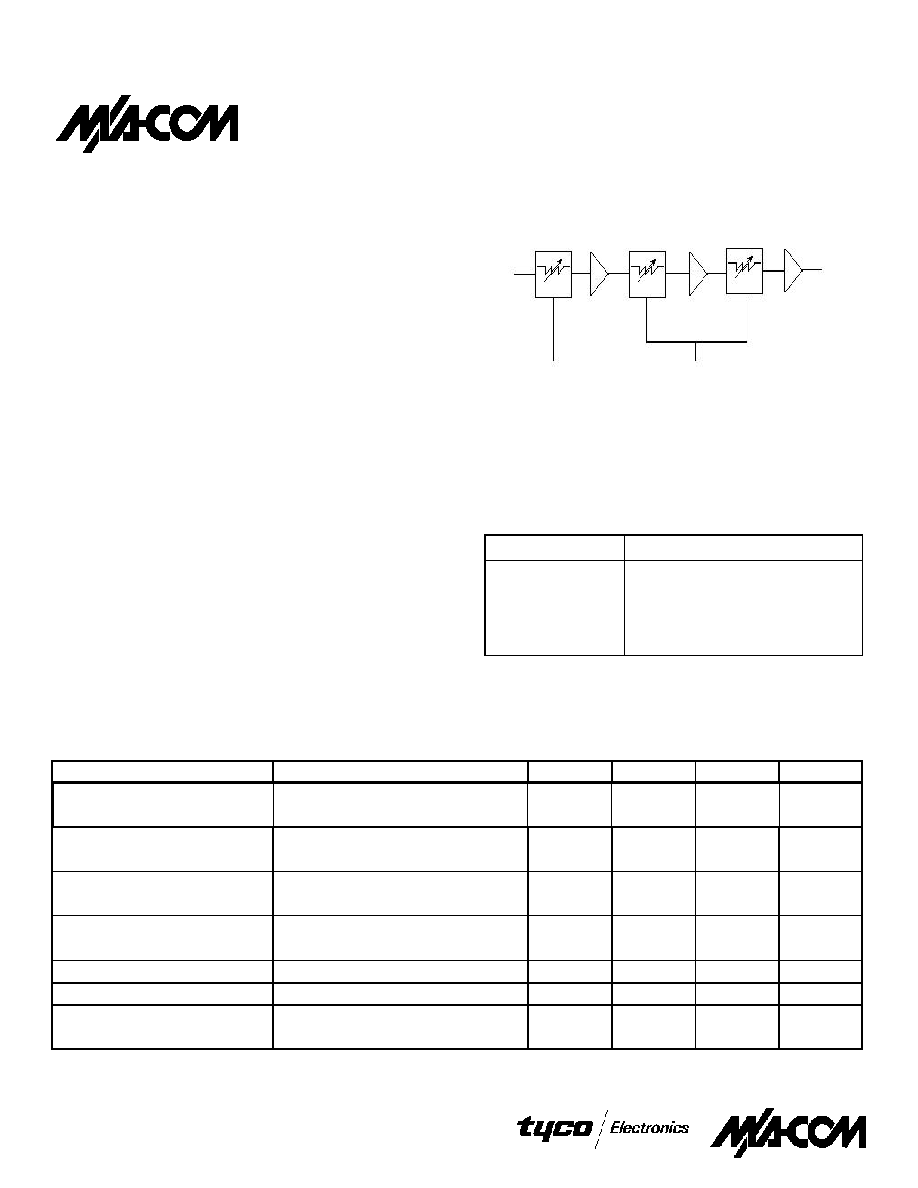
VCTL2
VCTL1
RF Out
RF In
Ordering Information
Part Number
Package
AM55-0023
FQFP-N 5.0 mm Plastic Package
AM55-0023TR
Forward Tape and Reel
1
AM55-0023RTR
Reverse Tape and Reel
1
AM55-0023SMB
Sample Board
1. If specific reel size is required, consult factory for part number
assignment.
Features
�
Highly Integrated Variable Voltage Gain Control Amplifier
�
Operates with 3.0 V to 5 V Supply Voltage
�
Greater than 40 dB dynamic range
�
High Output P
1dB
: +17 dBm @ 3 V, 19 dBm @ 5V
�
Low Cost 5 mm FQFP-N Package
Description
M/A-COM's AM55-0023 is a high performance, voltage
controlled, variable gain amplifier. It has been designed for use
in a broad range of applications including cellular base stations
and mobile radio where AGC is required to increase system
dynamic range.
The gain control operates best in the 900 MHz range and also
has useable gain to 2.5 GHz. DC current is low at 160 mA at
3V bias and 200 mA at 5V bias. The package is a low cost
MLF.
The AM55-0023 is fabricated using M/A-COM's 0.5 micron
low noise GaAs MESFET process. The process features full
passivation for performance and reliability.
AM55-0023
Variable Voltage Gain Control Amplifier
0.8 - 2.0 GHz
1
Electrical Specifications T
A
= +25� C
Parameter
Test Conditions
Units
Min.
Typ.
Max.
Gain
Frequency = 0.9 GHz
dB
23
25
Frequency = 2.0 GHz
dB
10
12
Attenuation Range
Frequency = 0.9 GHz
dB
40
44
Frequency = 2.0 GHz
dB
37
41
I/P Return Loss
Frequency = 0.9 GHz
dB
14
17
Frequency = 2.0 GHz
dB
7
10
O/P Return Loss
Frequency = 0.9 GHz
dB
11
14
Frequency = 2.0 GHz
dB
10
13
Noise Figure (min attn)
Frequency = 0.9 GHz
dB
9
12
P
1dB
Max P
1dB
when V
DDB1,2,3
at 5 V
dBm
14
18
IMD
V
DDB
= 5 V
dB
29
32
V
DDA
= 5 V
dB
25
28
Functional Block Diagram

n
North America: Tel. (800) 366-2266, Fax (800) 618-8883
n
Asia/Pacific: Tel.+81-44-844-8296, Fax +81-44-844-8298
n
Europe: Tel. +44 (1344) 869 595, Fax+44 (1344) 300 020
Specifications subject to change without notice.
Visit www.macom.com for additional data sheets and product information.
V 2.0
Variable Voltage Gain Control Amplifier, 2.0 GHz
AM55-0023
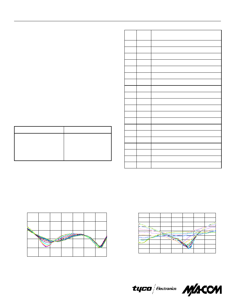
Pin Configuration
PIN
No.
PIN
Name
Description
1
Input
RF Input
2
NC
3
NC
4
NC
5
VCTL2
Second Attenuation Control
6
NC
7
NC
8
NC
9
VCTL1
First Attenuation Control
10
NC
11
NC
12
NC
13
Output
RF Output
14
VDDB3
Bias Pins
15
VDDA3
Bias Pins
16
VDDA2
Bias Pins
17
VDDB2
Bias Pins
18
VDDB1
Bias Pins
19
VDDA1
Bias Pins
20
NC
2
Operating Instructions
Two pins, VCTL1 and VCTL2 control the attenuation function
of this part. Varying these pins between 0 and 4.5 V controls the
attenuation. VCTL1 should be controlled first to avoid
degrading the input match and noise figure until more
attenuation is needed
. VCTL1 controls an attenuator with 30
dB of range and VCTL2 15dB of range.
The AM55-0023 has two sets of Vdd pins. VDDA1,2 ,3 and
VDDB1,2,3. VDDA should be supplied with 5 V. This voltage
is internally stepped down to 3 V to reduce current
consumption. If current consumption is not a concern OR only
3 V is available to the part then the VDDB pins should be used.
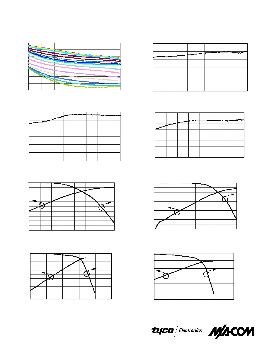
Using the VDDB pins with 5 V will also give greater IP3/IMD
performance (See graphs).
Note: When using one set of bias pins the other should be left
open circuited.
Typical Performance Curves
-25
-20
-15
-10
-5
0
0.6
0.8
1
1.2
1.4
1.6
1.8
2
FREQUENCY (GHz)
dB
Output Return Loss
(over full attenuation range
-45
-40
-35
-30
-25
-20
-15
-10
-5
0
0.6
0.8
1
1.2
1.4
1.6
1.8
2
FREQUENCY (GHz)
dB
Input Return Loss
(over full attenuation range)
Absolute Maximum Ratings
1
Parameter
Absolute Maximum
Input Power
2
+20 dBm
Operating Voltages
2
V
DDA/B1,2,3
= +6 volts
Operating Temperature
-40 �C to +85 �C
Storage Temperature
-65 �C to +150 �C
1. Exceeding any one or combination of these limits may cause
permanent damage.
2. Ambient Temperature (T
A
) = +25
�
C

n
North America: Tel. (800) 366-2266, Fax (800) 618-8883
n
Asia/Pacific: Tel.+81-44-844-8296, Fax +81-44-844-8298
n
Europe: Tel. +44 (1344) 869 595, Fax+44 (1344) 300 020
Specifications subject to change without notice.
Visit www.macom.com for additional data sheets and product information.
V 2.0
3
Variable Voltage Gain Control Amplifier, 2.0 GHz
AM55-0023
Typical Performance Curves (Cont'd)
0
5
10
15
20
25
30
35
40
0.5
0.6
0.7
0.8
0.9
1.0
1.1
1.2
1.3
FREQUENCY (GHz)
dB
Swept IMD (VDDB Pins at 5V)
0
5
10
15
20
25
30
0.5
0.6
0.7
0.8
0.9
1
1.1
1.2
1.3
FREQUENCY (GHz)
dB
Swept IMD (VDDA Pins at 5V)
0
2
4
6
8
10
12
0.4
0.6
0.8
1.0
1.2
1.4
FRQUENCY (GHz)
dB
Noise Figure
P
1dB
at 800 MHz (VDDA Pins 5V Supply)
0
2
4
6
8
10
12
14
16
18
20
-20
-18
-16
-14
-12
-10
-8
-6
PIN (dBm)
P
OUT
(dBm)
-6
-5
-4
-3
-2
-1
0
Relative Gain (dB)
0
2
4
6
8
10
12
14
16
18
20
-25
-20
-15
-10
-5
PIN (dBm)
P
OUT
(dBm)
-5
-4
-3
-2
-1
0
Relative Gain (dB)
P
1dB
at 900 MHz (VDDA Pins 5V Supply)
0
2
4
6
8
10
12
14
16
18
20
22
-25
-20
-15
-10
-5
0
PIN (dBm)
P
OUT
(dBm)
-5
-4
-3
-2
-1
0
Relative Gain (dB)
P
1dB
at 800 MHz (VDDB Pins 5V Supply)
-35
-25
-15
-5
5
15
25
35
0.6
0.8
1.0
1.2
1.4
1.6
1.8
2.0
FREQUENCY (GHz)
dB
Attenuation Range
P
1dB
at 900 MHz (VDDB Pins 5V Supply)
-5
0
5
10
15
20
25
-20
-15
-10
-5
0
PIN (dBm)
P
OUT
(dBm)
-3.5
-3
-2.5
-2
-1.5
-1
-0.5
0
Relative Gain (dB)

n
North America: Tel. (800) 366-2266, Fax (800) 618-8883
n
Asia/Pacific: Tel.+81-44-844-8296, Fax +81-44-844-8298
n
Europe: Tel. +44 (1344) 869 595, Fax+44 (1344) 300 020
Specifications subject to change without notice.
Visit www.macom.com for additional data sheets and product information.
V 2.0
4
Variable Voltage Gain Control Amplifier, 2.0 GHz
AM55-0023
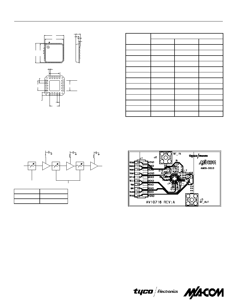
5 mm FQFP-N - 20
Measurement (mm)
Min.
Nom.
Max.
A
0.80
0.90
1.00
A1
0
0.02
0.05
A2
0
0.65
1.00
A3
0.25 ref.
b
0.23
0.30
0.38
D
5.00 basic
D1
4.75 basic
D2
1.25
2.70
3.25
e
0.65 basic
E
5.00 basic
E1
4.75 basic
E2
1.25
2.70
3.25
L
0.35
0.55
0.75
Dim.
5 mm FQFP-N - 20
1
E2
20 x b
e
4 x e
L
e
4 x e
D2
D
E
E1
D1
A
A2
A1
A3
1. See JEDEC MO-220A VHHC for additional dimensional and
tolerance information
External Components
1, 2
Component
Value
L
68nH
C
100pF
1. See Operating Instructions for details on VDD pins.
2. Requires 6 external components.
VCTL2
VCTL1
RFIN
RFOUT
VDDA/B
L
C
VDDA/B
L
C
VDDA/B
L
C
Sample Board
