UMTS Digital Gain Control
Amplifier, 1.94 - 2.34 GHz
AM55
-
0027
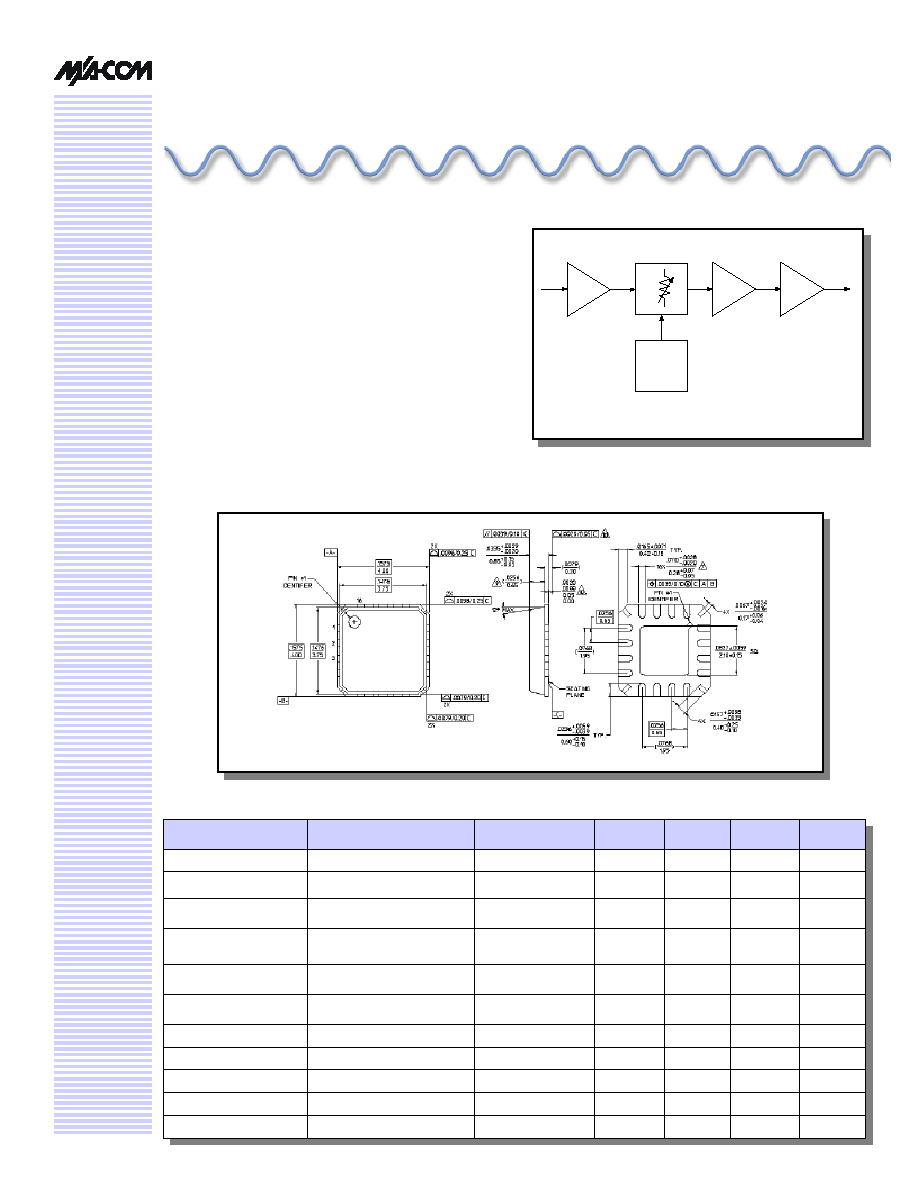
4mm FQFP-N Package Style
V 1E.00
Advanced
Features
n
Digitally Controlled Gain Block
n
Parallel Control Interface
n
4mm FQFP-N Package
n
Single Positive Supply Voltage
n
0.25 dB Steps of Attenuation
n
10 dB Atttenuation Range
Description
M/A-COM's AM55-0027 is a digitally controlled Variable
Gain Amplifier. Attenuation range is 10 dB with
Attenuation Steps of 0.25 dB. Attenuation is controlled
digitally through a parallel interface.
Electrical Specifications: T
A
= 25�C, Z
0
= 50
, V
S
= 5V
Parameter
Conditions
Frequency
Units
Min.
Typ.
Max.
Gain
No Attenuation
1.94 - 2.34 GHz
dB
24
26
--
Attenuation Range
--
1.94 - 2.34 GHz
dB
10
10
--
Attenuation Step Size
--
1.94 - 2.34 GHz
dB
0.2
0.25
0.3
Amplitude Flatness
--
All attenuation states
1.94 - 2.34 GHz
2.09 - 2.19 GHz
dB
dB
--
--
--
--
� 0.3
� 0.1
Input Return Loss
--
1.94 - 2.34 GHz
dB
13
18
--
Output Return Loss
--
1.94 - 2.34 GHz
dB
10
14
--
Output P1 dB
0 dB attenuation
1.94 - 2.34 GHz
dBm
15
19
--
Output IP3
0 dB attenuation
1.94 - 2.34 GHz
dBm
30
31
--
Noise Figure
0 dB attenuation
1.94 - 2.34 GHz
dB
--
4.7
--
Noise Figure
10 dB attenuation
1.94 - 2.34 GHz
dB
--
9.0
--
Supply Current
--
--
mA
--
110
120
Block Diagram
8 dB
Gain
IN
10 dB
Range
in
0.25 dB
Steps
8 dB
Gain
9 dB
Gain
OUT
Parallel
Control
Interface
UMTS Digital Gain Control Amplifier, 1.94 - 2.34 GHz
AM55-0027
Specifications subject to change without notice.
n
North America: Tel. (800) 366-2266
n
Asia/Pacific: Tel.+81-44-844-8296, Fax +81-44-844-8298
n
Europe: Tel. +44 (1344) 869 595, Fax+44 (1344) 300 020
Visit www.macom.com for additional data sheets and product information.
V 1E.00
2
Ordering Information
Part Number
Package
AM55-0027
Bulk Packaging
AM55-0027TR
Tape and Reel (1K Reel)
AM55-0027-TB
Units Mounted on Test Board
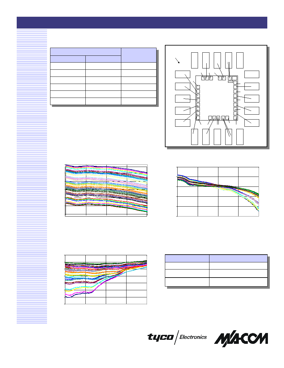
Typical Performance Curves
Input Return Loss vs. Frequency
Gain vs. Frequency
Output Return Loss vs. Frequency
15
17
19
21
23
25
27
1.94
2.04
2.14
2.24
2.34
Frequency (GHz)
S21 (dB)
-35
-30
-25
-20
-15
-10
1.94
2.04
2.14
2.24
2.34
Frequency (GHz)
S11 (dB)
-24
-22
-20
-18
-16
-14
-12
-10
1.94
2.04
2.14
2.24
2.34
Frequency (GHz)
S22 (dB)
Pin Out Table
Control Pin
5V
0V
Vcc6
0.25 dB
Vcc1
0.5 dB
Vcc2
1 dB
Vcc3
Vcc3N
2 dB
Vcc4
Vcc4N
4 dB
Vcc5
Vcc5N
8 dB
Attenuation
State
*All Vdd pins = 5V
Example: To get 7.5 dB Attenuation Vcc4 = 5V, Vcc4N = 0V,
Vcc3 = 5V, Vcc3N = 0V, Vcc2 = 5V and Vcc1 = 5V
Note: In this case Vcc5 = 0V therefore Vcc5N is 5V, and
Vcc6 = 0
Pin Out Figure
VCC6
N/C
VDD1
RF IN
N/C
N/C
RF OUT
VDD3
VDD2
N/C
VCC1
VCC3N
VDD
VCC5N
VCC4N
VCC4
VCC2
VCC5
VCC3
N/C
Pin #1
Pin #20