 | –≠–ª–µ–∫—Ç—Ä–æ–Ω–Ω—ã–π –∫–æ–º–ø–æ–Ω–µ–Ω—Ç: AM59-0029 | –°–∫–∞—á–∞—Ç—å:  PDF PDF  ZIP ZIP |
250 mW S-Band Power Amplifier,
2.2 - 2.4 GHz
AM59
-
0029
OUTLINE DRAWING
V 1P.00
Preliminary
Features
∑
High Linear Gain: 29 dB typ.
∑
High Saturated Output Power: +24 dBm typ.
∑
50 Ohm Input/Output Matched
∑
InGaP HBT Process
Description
M/A-COM's AM59-0029 is a two-stage MMIC power
amplifier available in a 4mm FQFP-16 plastic package.
The AM59-0029 has fully matched input and output net-
works. The AM59-0029 is designed to operate from a
constant voltage collector supply. By varying the bias
conditions, the saturated output power performance of
this device may be tailored for various applications.
The AM59-0029 is ideally suited for use as an output
stage in telemetry systems. The AM59-0029 requires
only supply line bypassing, minimizing the number of
external components required.
M/A-COM's AM59-0029 is fabricated using an InGaP
HBT process. The process features full passivation for
increased performance and reliability. This product is 100%
RF tested to ensure compliance to performance
specifications.
Electrical Specifications: Vcc = +3V, Zo = 50 Ohms, T
A
= 25∞C
Parameter
Test Conditions
Frequency
Units
Min
Typ
Max
Linear Gain
Pin = -20 dBm
2.2 - 2.4 GHz
dB
--
29
--
Input VSWR
Pin = -20 dBm
2.2 - 2.4 GHz
Ratio
--
--
2.0:1
Output VSWR
Pin = -20 dBm
2.2 - 2.4 GHz
Ratio
--
--
2.0:1
Output Power
(Saturated)
Pin = +10 dBm
2.2 - 2.4 GHz
dBm
--
24
--
Output Power vs.
Frequency
Pin = +10 dBm
2.2 - 2.4 GHz
dB
--
--
± 0.4
Output Power vs.
Temperature
T
A
= -40∞C to +85∞C,
Pin = +10 dBm
2.2 - 2.4 GHz
dB
--
--
± 0.8
Collector Bias Current
Pin = +10 dBm
2.2 - 2.4 GHz
mA
--
400
--
Base Bias Current
Pin = +10 dBm
2.2 - 2.4 GHz
mA
--
5
--
Power Added Efficiency
Pin = +10 dBm
2.2 - 2.4 GHz
%
--
22
--
250 mW S-Band Power Amplifier, 2.2 - 2.4 GHz
AM59-0029
V 1P.00
M/A-COM Inc. and its affiliates reserve the right to make changes to the product(s)
or information contained herein without notice. M/A-COM makes no warranty,
representation, or guarantee regarding the suitability of its products for any particular
purpose, nor does M/A-COM assume any liability whatsoever arising out of the use
or application of any product(s) or information.
Visit www.macom.com for additional data sheets and product information.
n
North America: Tel. (978) 656-2693
n
Asia/Pacific: Tel.+81-44-844-8296, Fax +81-44-844-8298
n
Europe: Tel. +44 (1344) 869 595, Fax+44 (1344) 300 020
2
Absolute Maximum Ratings
1,2
1. Operation of this device above any one of these
parameters may cause permanent damage.
2. Adequate heat sinking and grounding required.
Parameter
Absolute Maximum
Input Power
+13 dBm
V
CC
+12 volts
V
BB
-8 volts to +6 volts
I
CC
600 mA
Max. Dissipation Power
1350 mW
Channel Temperature
+150∞C
Operating Temperature
-40∞C to +85∞C
Storage Temperature
-65∞C to +150∞C
3. Apply +3 volts V
CC
. Adjust V
BB
by changing the resis-
tors, R6 and R7, for desired base current.
4. For optimum IP3 performance, V
CC
bypass capacitors
should be placed within 0.5 inches of the V
CC
leads.
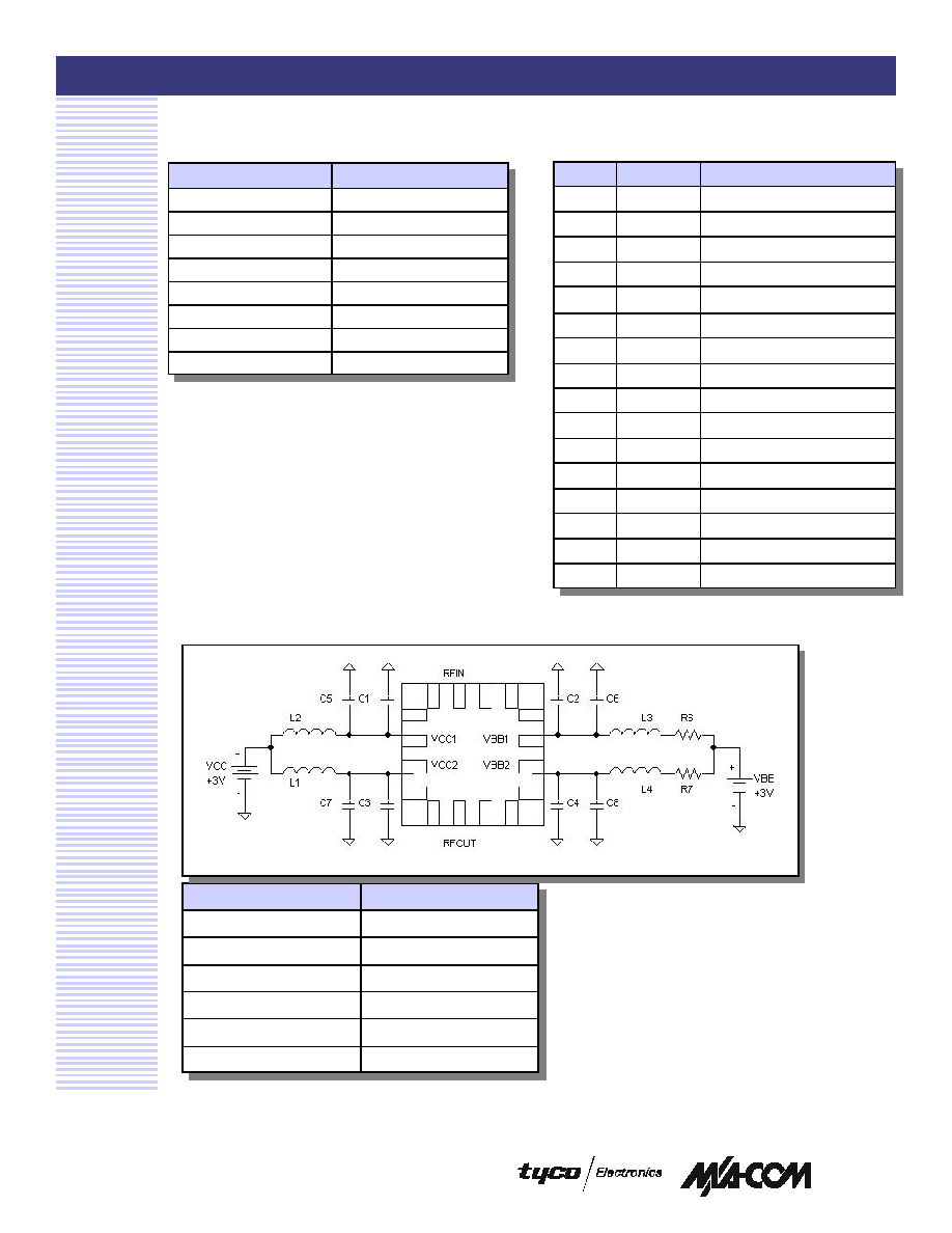
Recommended Bias Configuration
3,4
Component
Value
R6
3.9K Ohm
R7
301 Ohm
L1, L2
68 nH
L3, L4
220 nH
C1,C2,C3,C4
100 pF
C5,C6,C7,C8
0.1 µF
Pin Configuration
Pin No.
Pin Name
Function
1
GND
GND
2
RF In
RF Input
3
GND
GND
4
GND
GND
5
GND
GND
6
VC1
Collector Supply to Stage 1
7
VC2
Collector Supply to Stage 2
8
GND
GND
9
GND
GND
10
RF Out
RF Output
11
GND
GND
12
GND
GND
13
GND
GND
14
VB2
Base Supply to Stage 2
15
VB1
Base Supply to Stage 2
16
GND
GND
250 mW S-Band Power Amplifier, 2.2 - 2.4 GHz
AM59-0029
V 1P.00
M/A-COM Inc. and its affiliates reserve the right to make changes to the product(s)
or information contained herein without notice. M/A-COM makes no warranty,
representation, or guarantee regarding the suitability of its products for any particular
purpose, nor does M/A-COM assume any liability whatsoever arising out of the use
or application of any product(s) or information.
Visit www.macom.com for additional data sheets and product information.
n
North America: Tel. (978) 656-2693
n
Asia/Pacific: Tel.+81-44-844-8296, Fax +81-44-844-8298
n
Europe: Tel. +44 (1344) 869 595, Fax+44 (1344) 300 020
3
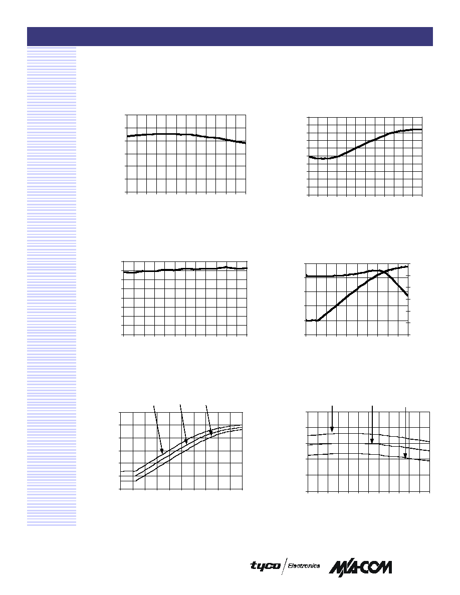
Output Power and ICC vs. Input
Power
Output Power vs. Input Power and
Temperature
Linear Gain vs. Frequency and
Temperature
Typical Performance Curves
VSWR vs. Frequency
Linear Gain vs. Frequency
Saturated Output Power vs.
Frequency (PIN = +10 dBm)
20
22
24
26
28
30
32
2.00
2.10
2.20
2.30
2.40
2.50
2.60
FREQUENCY (GHz)
LINEAR GAIN (dB)
1.0
1.1
1.2
1.3
1.4
1.5
1.6
1.7
1.8
1.9
2.0
2.00
2.10
2.20
2.30
2.40
2.50
2.60
FREQUENCY (GHz)
VSWR
10
12
14
16
18
20
22
24
26
2.00
2.10
2.20
2.30
2.40
2.50
2.60
FREQUENCY (GHz)
OUTPUT POWER (dBm)
0
5
10
15
20
25
-20 -17 -14 -11 -8
-5 -2
1
4
7
10
INPUT POWER (dBm)
OUTPUT POWER (dBm)
330
344
358
372
386
400
414
CURRENT (mA)
0
5
10
15
20
25
30
-20 -17 -14 -11
-8
-5
-2
1
4
7
10
INPUT POWER (dBm)
OUTPUT POWER (dBm)
-40∞C
+25∞C
+85∞C
20
23
26
29
32
35
2.00
2.10
2.20
2.30
2.40
2.50
2.60
FREQUENCY (GHz)
LINEAR GAIN (dB)
-40∞C
+25∞C
+85∞C
250 mW S-Band Power Amplifier, 2.2 - 2.4 GHz
AM59-0029
V 1P.00
M/A-COM Inc. and its affiliates reserve the right to make changes to the product(s)
or information contained herein without notice. M/A-COM makes no warranty,
representation, or guarantee regarding the suitability of its products for any particular
purpose, nor does M/A-COM assume any liability whatsoever arising out of the use
or application of any product(s) or information.
Visit www.macom.com for additional data sheets and product information.
n
North America: Tel. (978) 656-2693
n
Asia/Pacific: Tel.+81-44-844-8296, Fax +81-44-844-8298
n
Europe: Tel. +44 (1344) 869 595, Fax+44 (1344) 300 020
4
Ordering Information
Part Number
Package
AM59-0029
FQFP-16 4mm
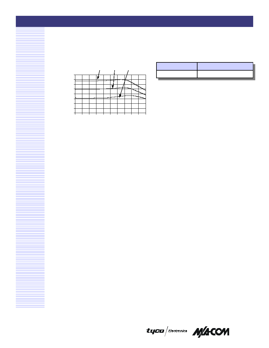
Typical Performance Curves
Collector Current vs. Input Power
and Temperature
300
320
340
360
380
400
420
440
460
-20 -17 -14 -11 -8
-5
-2
1
4
7 10
INPUT POWER (dBm)
CURRENT (mA)
-40∞C
+25∞C
+85∞C