Voltage Variable Absorptive
Attenuator, 800 - 1000 MHz
AT10
-
0009
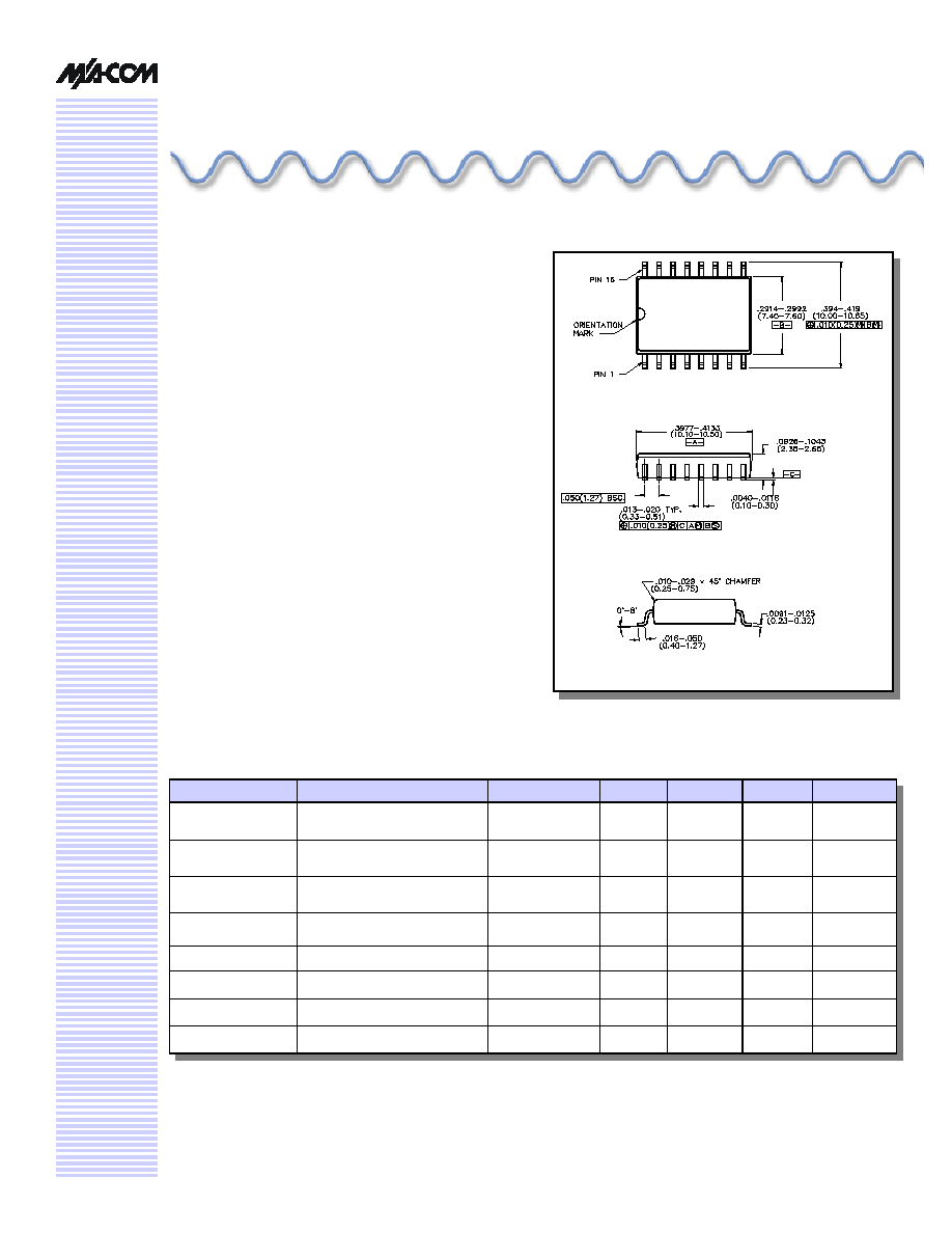
SOW-16
V 7.00
Features
n
Input IP3: +31 dBm Min. (Full Attenuation Range)
n
Input IP3 is 15 -20 dB Better Than GaAs
n
Linear Operation: +20 dBm Min.
n
Plastic SOIC, Wide Body, SMT Package
n
38 dB Dynamic Range (With 30 mA Bias Current)
n
Single Control Voltage
n
50 ohm Impedance
n
Linear Driver, DR65-0002, Available
n
Test Boards are Available
n
Tape and Reel Packaging Available
Description
M/A-COM's AT10-0009 is a PIN diode based voltage
variable attenuator. This device is in a SOIC-16, wide body
plastic surface mount package. These attenuators have
linear operating power and input intercept point levels
15 - 20 dB better than GaAs FET MMIC voltage variable
attenuators. They are ideally suited for use where low
distortion, high linear operating power and high dynamic
range are required. These devices are optimized for the
GSM frequency band, but exhibit excellent performance
and repeatability over the entire specified frequency band.
The AT10-0009 is ideally suited for wireless
communications systems.
Electrical Specifications: T
A
= 25∞C
Parameter
Test Conditions
Frequency
Units
Min
Typical
Max
Insertion Loss
0 volts
800-1000 MHz
925 - 960 MHz
dB
dB
--
--
3.5
3.3
4.2
3.9
Attenuation
(Above Loss)
12 mA bias current
800-1000 MHz
925 - 960 MHz
dB
dB
30
33
-
38
--
--
Frequency
Flatness
0 to 30 dB attenuation
800-1000 MHz
925 - 960 MHz
dB
dB
--
--
1.5
0.4
2.5
0.8
VSWR
0 to 30 dB attenuation
800-1000 MHz
925 - 960 MHz
Ratio
Ratio
--
--
1.6:1
1.4:1
2.0:1
1.7:1
Switching Speed
50% Control to 90%/10% RF
800-1000 MHz
µs
--
--
10.0
Linear Operation
--
800-1000 MHz
dBm
--
+20
--
Input IP
3
Two-tone inputs up to +10 dBm
800-1000 MHz
dBm
+35
+40
---
I
Control
--
800-1000 MHz
mA
--
--
30
Package outline conforms to JEDEC standard MS-013AA.
Voltage Variable Absorptive Attenuator, 800 - 1000 MHz
AT10-0009
Specifications subject to change without notice.
n
North America: Tel. (800) 366-2266
n
Asia/Pacific: Tel.+81-44-844-8296, Fax +81-44-844-8298
n
Europe: Tel. +44 (1344) 869 595, Fax+44 (1344) 300 020
Visit www.macom.com for additional data sheets and product information.
V 7.00
2
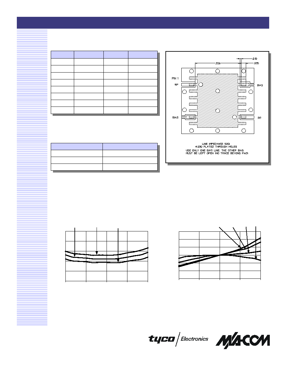
Recommended PCB Configuration
Pin Configuration
Pin #
Function
Pin #
Function
1
GND
9
GND
2
RF
10
RF
3
GND
11
GND
4
GND
12
GND
5
GND
13
GND
6
GND
14
GND
7
Bias
2
15
Bias
2
8
GND
16
GND
2. Bias currents may be applied to pin 7 or 15. The unused pin
should be isolated.
Typical Performance Curves
Attenuation Flatness (dB) @ +25∞C
Insertion Loss
1
2
3
4
5
6
750
825
900
975
1050
Frequency (MHz)
Loss (dB)
+25∞C
+85∞C
-40∞C
-3
-2
-1
0
1
2
3
750
825
900
975
1050
Frequency (MHz)
Flatness (dB)
30 dB
20 dB
10 dB Ref
1. Operation of this device above any one of these parameters
may cause permanent damage.
Parameter
Absolute Maximum
Max. Input Power
+27 dBm
Operating Temperature
-40∞C to +85∞C
Storage Temperature
-65∞C to +125∞C
Absolute Maximum Ratings
1
Voltage Variable Absorptive Attenuator, 800 - 1000 MHz
AT10-0009
Specifications subject to change without notice.
n
North America: Tel. (800) 366-2266
n
Asia/Pacific: Tel.+81-44-844-8296, Fax +81-44-844-8298
n
Europe: Tel. +44 (1344) 869 595, Fax+44 (1344) 300 020
Visit www.macom.com for additional data sheets and product information.
V 7.00
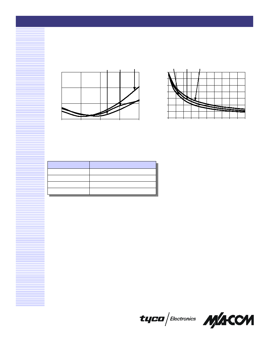
Typical Performance Curves
Attenuation vs. Bias Current
Typical VSWR @ +25∞C
3
Part Number
Package
AT10-0009
Tube
AT10-0009TR
Tape and Reel (1K Reel)
AT10-0009-TB
Unit Mounted on Test Board
DR65-0002-TBG
Unit with Driver on Test Board
Ordering Information
1.0
1.5
2.0
2.5
750
825
900
975
1050
Frequency (MHz)
VSWR (Ratio)
Ref
30 dB
15 dB
-42
-36
-30
-24
-18
-12
-6
0
0
1
2
3
4
5
6
7
8
9
10
Bias Current (mA)
Attenuation (dB)
+85∞C
+25∞C
-40∞C