 | –≠–ª–µ–∫—Ç—Ä–æ–Ω–Ω—ã–π –∫–æ–º–ø–æ–Ω–µ–Ω—Ç: AT-106 | –°–∫–∞—á–∞—Ç—å:  PDF PDF  ZIP ZIP |
Digital Attenuator, 50 dB, 6-Bit,
TTL Driver, DC - 2 GHz
AT
-
106
CR-13
V 5.00
Features
n
Attenuation: 1 dB steps to 50 dB
n
Temperature Stability: ± 0.18 dB from ≠55∞C to +85∞C
Typical
n
Low DC Power Consumption
n
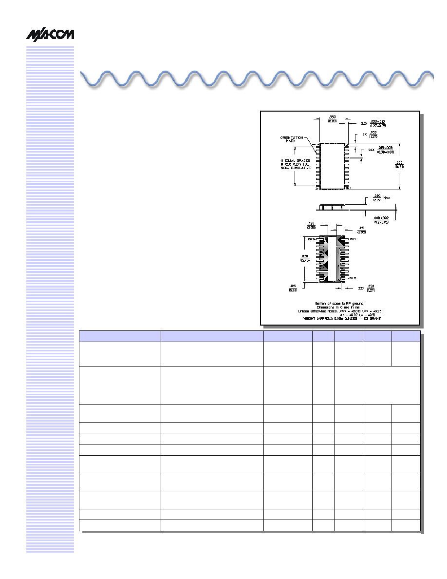
Hermetic Surface Mount Package
n
Integral TTL Driver
n
50 Ohm Nominal Impedance
Description
M/A-COM's AT-106 is a GaAs FET 6-bit digital attenuator
with a 1 dB minimum step size and 50 dB total attenuation.
This attenuator and integral TTL driver is in a hermetically
sealed ceramic 24-lead surface mount package. The AT-
106 is ideally suited for use where accuracy, fast switching,
very low power consumption and low intermodulation
products are required. Typical applications include dy-
namic range setting in precision receiver circuits and other
gain/leveling control circuits. Environmental screening is
available. Contact the factory for information.
Electrical Specifications
1
(From ≠55∞C to +85∞C)
Parameter
Test Conditions
Frequency
Units
Min
Typ
Max
Reference Insertion Loss
--
DC - 0.5 GHz
DC - 1.0 GHz
DC - 2.0 GHz
dB
dB
dB
--
--
--
--
--
--
3.6
4.1
4.6
Attenuation Accuracy
2
Any Single Bit
Any Combination of Bits
(For attenuation to 26 dB)
Any Combination of Bits
(For attenuation 27 to 50 dB)
DC - 2.0 GHz
DC - 2.0 GHz
DC - 1.5 GHz
dB
dB
dB
± (0.3 +4% of atten. setting)
± (0.4 +4% of atten. setting)
± (0.5 +5% of atten. setting)
VSWR
--
0.05 - 0.10 GHz
0.101 - 2.0 GHz
Ratio
Ratio
--
--
--
--
2.0:1
1.8:1
Trise, Tfall
10% to 90%
--
ns
--
9
--
Ton, Toff
50% Control to 90/10% RF
--
ns
--
45
--
Transients
In-Band (peak-peak)
--
mV
--
40
--
1 dB Compression
Input Power
Input Power
0.05 GHz
0.5 - 2.0 GHz
dBm
dBm
--
--
+20
+28
--
--
Input IP3
For two-tone Input Power
Up to +5 dBm
0.05 GHz
0.5 - 2.0 GHz
dBm
dBm
--
--
+34
+46
--
--
Input IP2
For two-tone Input Power
Up to +5 dBm
0.05 GHz
0.5 - 2.0 GHz
dBm
dBm
--
--
+75
+79
--
--
Vcc
--
--
V
4.5
5.0
5.5
Vee
--
--
V
-8.0
--
-5.0
1. All specifications apply when operated with bias voltages of +5V for Vcc and ≠5.0V for Vee.
2. This attenuator is guaranteed monotonic.
Digital Attenuator, 50 dB, 6-Bit, TTL Driver, DC - 2 GHz
AT-106
Specifications subject to change without notice.
n
North America: Tel. (800) 366-2266
n
Asia/Pacific: Tel.+81-44-844-8296, Fax +81-44-844-8298
n
Europe: Tel. +44 (1344) 869 595, Fax+44 (1344) 300 020
Visit www.macom.com for additional data sheets and product information.
V 5.00
2
Parameter
Test Conditions
Frequency
Units
Min
Typ
Max
Icc
Vcc = 4.5 to 5.5V
Vctl = 0 to 0.8V, or Vcc ≠2.1V to Vcc
--
mA
--
--
6.0
Iee
Vee = -5.0 to -8.0V
--
mA
--
--
1.0
Vctl
Vctl
Logic 0 (TTL)
Logic 1 (TTL)
--
--
V
V
0.0
2.0
--
--
0.8
5.0
Input Leakage Current (Low)
0 to 0.8V
--
µA
--
--
1.0
Input Leakage Current (High)
2.0 to 5.0V
--
µA
--
--
1.0
Electrical Specifications (From ≠55∞C to +85∞C)
Absolute Maximum Ratings
3
3. Operation of this device above any one of these parameters
may cause permanent damage.
4. Standard CMOS TTL interface, latch-up will occur if logic
signal is applied prior to power supply.
Parameter
Absolute Maximum
Max Input Power
0.5 GHz
0.5 - 2.0 GHz
+27 dBm
+34 dBm
Supply Voltages
Vcc
Vee
+5.5V
-8.5V
Control Voltage
4
-0.5V to Vcc +0.5V
Operating Temperature
-55∞C to +125∞C
Storage Temperature
-65∞C to +150∞C
Truth Table
C6
C5
C4
C3
C2
C1
Attenuation
0
0
0
0
0
0
Reference
0
0
0
0
0
1
1 dB
0
0
0
0
1
0
2 dB
0
0
0
1
0
0
4 dB
0
0
1
0
0
0
8 dB
0
1
0
0
0
0
16 dB
1
0
0
0
0
0
32 dB
1
1
1
1
1
1
63 dB
Control Inputs
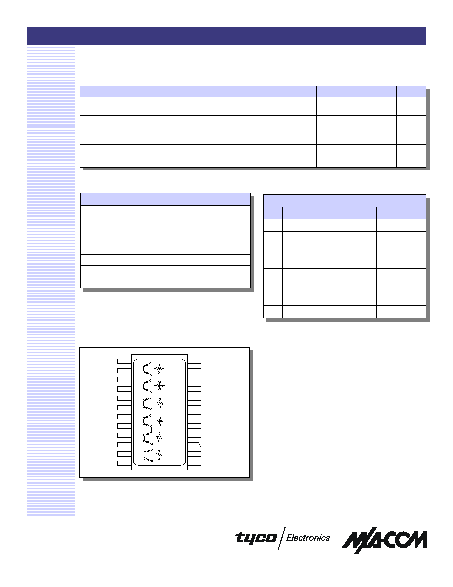
Functional Schematic (Top View)
PIN 1 GND
GND
GND
C32
C16
Vee (-5V to -8V)
Vcc (+5V)
C8
GND
GND
GND
GND
GND
GND
RF1 PIN 24
32 dB
16 dB
8 dB
4 dB
2 dB
1 dB
GND
GND
GND Orientation Mark
GND
RF2 PIN 13
C4
C2
C1
PIN 12 GND
0 = TTL Low 1 = TTL High
Digital Attenuator, 50 dB, 6-Bit, TTL Driver, DC - 2 GHz
AT-106
Specifications subject to change without notice.
n
North America: Tel. (800) 366-2266
n
Asia/Pacific: Tel.+81-44-844-8296, Fax +81-44-844-8298
n
Europe: Tel. +44 (1344) 869 595, Fax+44 (1344) 300 020
Visit www.macom.com for additional data sheets and product information.
V 5.00
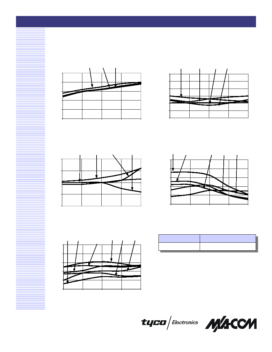
Typical Performance Curves
Attenuation Accuracy vs. Frequency
Insertion Loss vs. Frequency
Attenuation Accuracy vs. Frequency
3
RF1 VSWR vs. Frequency
RF2 VSWR vs. Frequency
Ordering Information
Part Number
Package
AT-106 PIN
CR-13
0
1
2
3
4
5
0.0
0.5
1.0
1.5
2.0
Frequency (GHz)
Insertion Loss (dB)
+85∞C
+25∞C
-55∞C
-0.60
-0.40
-0.20
0.00
0.20
0.40
0.60
0.0
0.5
1.0
1.5
2.0
Frequency (GHz)
Deviation from Nominal Atten
(dB)
1 dB
2 dB
4 dB
8 dB
-2.00
-1.00
0.00
1.00
2.00
0.0
0.5
1.0
1.5
2.0
Frequency (GHz)
Deviation from Nominal Atten (dB)
16 dB
32 dB
40 dB
50 dB
1
1.2
1.4
1.6
1.8
2
0.0
0.5
1.0
1.5
2.0
Frequency (GHz)
VSWR
1 dB
4 dB
8 & 16 dB
32 dB
Ref Loss & 2 dB
1
1.2
1.4
1.6
1.8
2
0.0
0.5
1.0
1.5
2.0
Frequency (GHz)
VSWR
1 dB
2 dB
8 dB
16 dB
Ref Loss
& 4 dB
32 dB