 | –≠–ª–µ–∫—Ç—Ä–æ–Ω–Ω—ã–π –∫–æ–º–ø–æ–Ω–µ–Ω—Ç: AT-108RTR | –°–∫–∞—á–∞—Ç—å:  PDF PDF  ZIP ZIP |
Features
∑
Single Positive Voltage Control 0 to +5 Volts
∑
40 dB Attenuation Range at 900 MHZ GHz
∑
± 2 dB Linearity from BSL
∑
Low DC Power Consumption
∑
Low-Cost SOIC-8 Plastic Package
∑
Tape and Reel Packaging Available
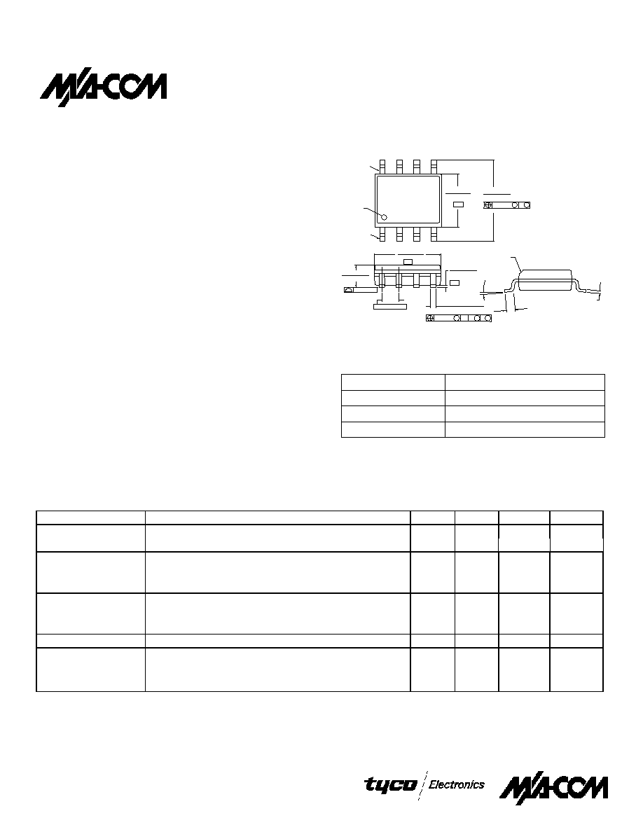
SOIC-8
1
Electrical Specifications: T
A
= 25∞C
1
=
=
=
=
Description
M/A-COM's AT-108 is a GaAs, MESFET MMIC voltage
variable absorptive attenuator in a low cost SOIC-8 lead surface
mount plastic package. The AT-108 is ideally suited for use
where linear attenuation fine tuning and very low power
consumption are required. Typical applications include radio,
cellular, GPS equipment and automatic gain/level control
circuits.
The AT-108 is fabricated with a monolithic GaAs MMIC using
a mature 1-micron process. The process features full chip
passivation for increased performance and reliability.
Ordering Information
Part Number
Package
AT-108
SOIC-8 Lead Plastic Package
AT-108TR
Forward Tape and Reel
1
AT-108RTR
Reverse Tape and Reel
1
Parameter
Test Conditions
1
Units
Min.
Typ.
Max.
Insertion Loss
0.5 - 1.0 GHz
dB
2.5
2.7
1.0 - 3.0 GHz
dB
3.2
3.5
Attenuation
0.5 - 1.0 GHz
dB
40
1.0 - 2.0 GHz
dB
35
2.0 - 3.0 GHz
dB
28
Flatness
0.5 - 1.0 GHz
dB
±0.5
±0.8
(Peak-to-Peak)
1.0 - 2.0 GHz
dB
±1.2
±1.5
2.0 - 3.0 GHz
dB
±1.5
±1.8
VSWR
0.5 - 3.0 GHz
2:1
T
rise
, T
fall
10% to 90% RF, 90% to 10% RF
µs
15
T
on
, T
off
50% Control to 90% RF, Control to 10% RF
µs
25
Transients
In-band
mV
12
1. All measurements in a 50
system.
1. If specific reel size is required, consult factory for part number
assignment.
(.19/.25)
CHAMFER
(OPTIONAL
)
(0.40/1.27)
.016/.050
0∞/80∞
-B-
BSC.
-C-
-A-
.010(.25) C A B
M
M S
.050 (1.27)
Oreintation
Mark
.1497/.1574
(3.80/4.00)
M
M B
.010(.25)
.2284/.2440
(5.80/6.20)
.0532/.0688
(1.35/1.75)
.004 (0.10)
.0075/.0098
PIN 8
PIN 1
.013/.020 (8
PL)
(.33/.51)
.0040/.0098
(.10/.25)
.1890/.1968
(4.80/5.00)
1. Dimensions are in inches/mm.
AT-108
Voltage Variable Absorptive Attenuator
Voltage Variable Absorptive Attenuator
Voltage Variable Absorptive Attenuator
Voltage Variable Absorptive Attenuator
40 dB, 0.5
40 dB, 0.5
40 dB, 0.5
40 dB, 0.5--
--
--
--3.0 GHz
3.0 GHz
3.0 GHz
3.0 GHz
North America: Tel. (800) 366-2266, Fax (800) 618-8883
Asia/Pacific: Tel.+81-44-844-8296, Fax +81-44-844-8298
Europe: Tel. +44 (1344) 869 595, Fax+44 (1344) 300 020
Specifications subject to change without notice.
Visit www.macom.com for additional data sheets and product information.
V 4.0
-2.8
-2.6
-2.4
-2.2
-2
-1.8
-1.6
0
0.5
0.66
0.82
0.97
1.13
1.28
1.44
1.6
1.75
1.91
2.06
2.22
2.38
2.53
2.69
2.84
Frequency (GHz)
Inser
tion Loss (dB
)
-25
-20
-15
-10
-5
0
5
4.5
4
3.5
3
2.5
2
1.5
1
0.5
0
Control Voltage (Volts)
R
e
tur
n
Loss (dB
)
Output RL
Input RL
-35
-30
-25
-20
-15
-10
-5
0
5
4.5
4
3.5
3
2.5
2
1.5
1
0.5
0
Control Voltage (Volts)
R
e
tu
rn
L
o
s
s
(d
B
)
Output RL
Input RL
-50
-45
-40
-35
-30
-25
-20
-15
-10
-5
0
5
4.5
4
3.5
3
2.5
2
1.5
1
0.5
0
Control Voltage (Volts)
A
ttenuation (dB
)
1800MHz
2200MHz
900MHz
Typical Performance Curves
Parameter
Absolute Maximum
Maximum Input Power
+21 dBm
Supply Voltage V
CC
-1V, +8V
Control Voltage V
C
-1V, V
CC
+ 0.5V
Operating Temperature
-40∞C to +85∞C
Storage Temperature
-65∞C to +150∞C
Absolute Maximum Ratings
1
1. Operation of this device above any one of these parameters
may cause permanent damage.
Attenuation vs. Control Voltage @ +25∞C
Insertion Loss vs. Frequency
Functional Schematic
8
7
6
5
1
3
2
4
G N D
R F
G N D
V c
G N D
G N D
R F
V cc
PIN
Orientation Mark
1. V
CC
= +5 V
DC
@ 50 µA max.
2. V
C
= 0 V
DC
to +5 V
DC
@ 50 µA max.
3. External DC blocking capacitors are required on all RF ports.
4. 39pF used for data measurements.
Return Loss vs. Control Voltage @ +25∞C
F = 900 MHz
Return Loss vs. Control Voltage @ +25∞C
F = 1800 MHz
Voltage Variable Absorptive Attenuator, 40 dB, 0.5-3.0 GHz
AT-108
North America: Tel. (800) 366-2266, Fax (800) 618-8883
Asia/Pacific: Tel.+81-44-844-8296, Fax +81-44-844-8298
Europe: Tel. +44 (1344) 869 595, Fax+44 (1344) 300 020
Specifications subject to change without notice.
Visit www.macom.com for additional data sheets and product information.
V 4.0
0
5
10
15
20
25
30
35
0
1
2
3
4
5
Control Voltage (Volts)
IP
3
(dB
m
)
-5
0
5
10
15
20
25
0
1
2
3
4
5
Control Voltage (Volts)
C
o
mpres
s
i
on P
o
i
n
t (dB
m
)
-2
-1
0
1
2
3
0
1
2
3
4
5
Control Voltage (Volts)
A
ttenuation D
e
lta (dB
)
-45
-40
-35
-30
-25
-20
-15
-10
-5
0
5
4.5
4
3.5
3
2.5
2
1.5
1
0.5
0
Control Voltage(Volts)
Atte
nua
ti
on (dB)
-45
-40
-35
-30
-25
-20
-15
-10
-5
0
5
4.5
4
3.5
3
2.5
2
1.5
1
0.5
0
Control Voltage(Volts)
A
ttenuation (dB
)
-50
-45
-40
-35
-30
-25
-20
0.
4
0.
56
0.
71
0.
87
1.
02
1.
18
1.
34
1.
49
1.
65
1.
8
1.
96
2.
12
2.
27
2.
43
2.
58
2.
74
2.
9
Frequency (dB)
A
ttenuation R
e
l to IL (dB
)
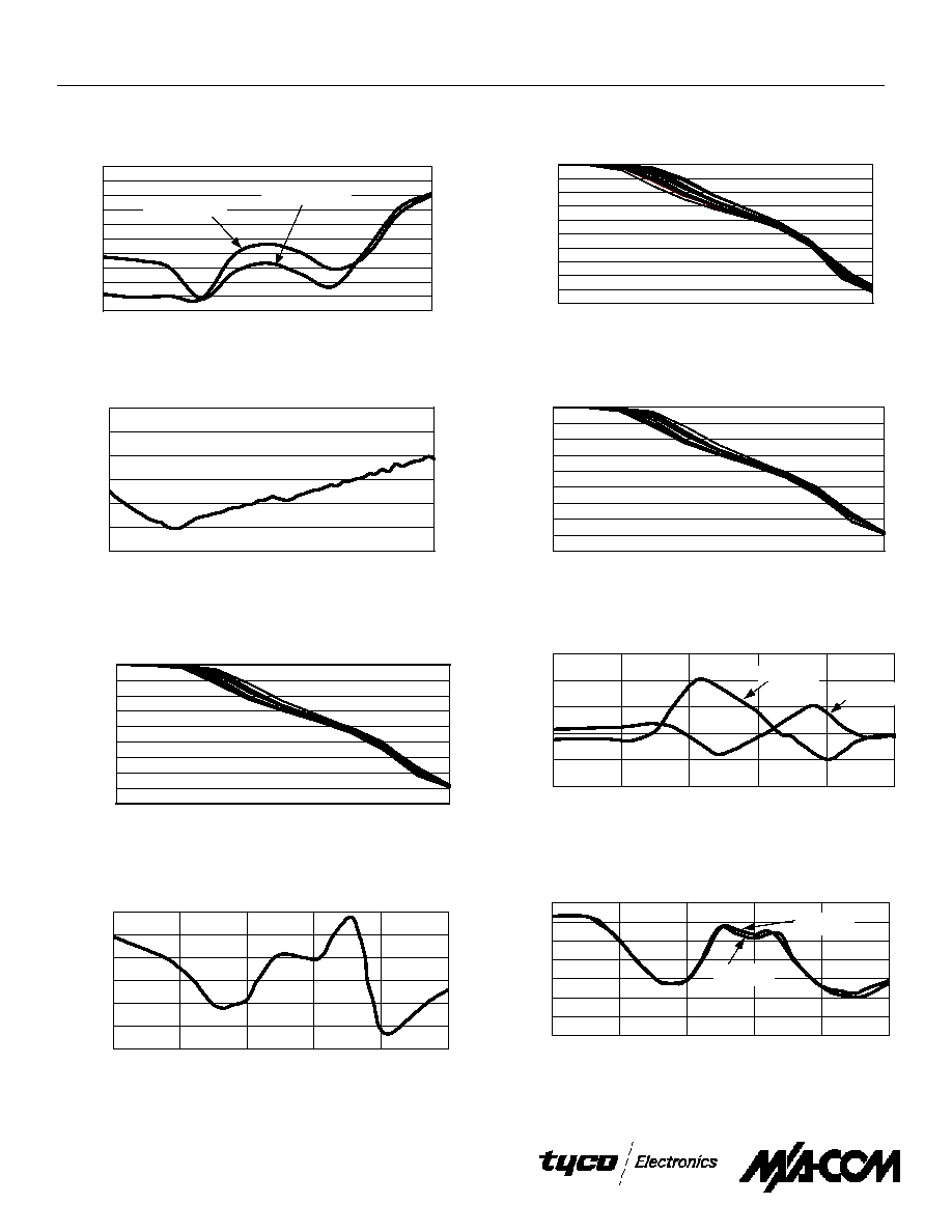
Typical Performance Curves (Cont'd)
Maximum Attenuation vs. Frequency
Attenuation vs. Control Voltage Typical
Device Deviations F = 2200 MHz @ +25∞C
Attenuation vs. Control Voltage Typical
Device Deviation F = 1800 MHz @ +25∞C
-50
-45
-40
-35
-30
-25
-20
-15
-10
-5
0
5
4.5
4
3.5
3
2.5
2
1.5
1
0.5
0
Control Voltage(Volts)
Atten
u
a
ti
o
n
(d
B)
-20
-18
-16
-14
-12
-10
-8
-6
-4
-2
0
5
4.5
4
3.5
3
2.5
2
1.5
1
0.5
0
Control Voltage (Volts)
R
e
tur
n
Loss (dB
)
Output Return Loss
Input Return Loss
Return Loss vs. Control Voltage @ +25∞C
F = 2200 MHz
Attenuation vs. Control Voltage Typical
Device Deviation f = 900 MHz @ +25∞C
Voltage Variable Absorptive Attenuator, 40 dB, 0.5-3.0 GHz
AT-108
North America: Tel. (800) 366-2266, Fax (800) 618-8883
Asia/Pacific: Tel.+81-44-844-8296, Fax +81-44-844-8298
Europe: Tel. +44 (1344) 869 595, Fax+44 (1344) 300 020
Specifications subject to change without notice.
Visit www.macom.com for additional data sheets and product information.
V 4.0
Attenuation vs. Temperature,
Normalized to +25∞C, F=900 MHz
-40∞C
-85∞C
1 dB Compression vs. Control Voltage
@ +25∞C, F = 900 MHz
IP
3
vs. Control Voltage
400 MHz
900 MHz