V 2.00
Part No.
Package
AT-109
SOIC 8-Lead Plastic Package
AT-109TR
Forward Tape & Reel*
AT-109RTR
Reverse Tape & Reel*
Parameter
Test Conditions
1
Unit
Min.
Typ.
Max
Insertion Loss
0.5 - 1.0 GHz
dB
2.5
2.7
1.0 - 2.0 GHz
dB
3.2
3.5
Attenuation
0.5 - 1.0 GHz
dB
35
1.0 - 2.0 GHz
dB
30
Flatness
0.5 - 1.0 GHz
dB
±0.5
±0.8
(Peak-to-Peak)
1.0 - 2.0 GHz
dB
±1.2
±1.5
VSWR
2:1
Trise, Tfall
10% to 90% RF, 90% to 10% RF
S
25
Ton, Toff
50% Control to 90% RF, Control to 10% RF
S
35
Transients
In-band
mV
12
F e a t u r e s
Single Positive Voltage Control 0 to +5 Vo l t s
35 dB Attenuation Range at 0.9 GHz
±2 dB Linearity from BSL
Low DC Power Consumption
Te m p e r a t u re Range: -40∞C to +85∞C
Low-Cost SOIC 8 Plastic Package
Tape and Reel Packaging Av a i l a b l e
D e s c r i p t i o n
M/A-COM's AT-109 is a GaAs MMIC voltage variable
absorptive attenuator in a low-cost SOIC 8-lead surf a c e
mount plastic package. The AT-109 is more linear than
the higher attenuation range AT-108. The AT-109 is ide-
ally suited for use where linear attenuation fine tuning
and very low power comsumption are re q u i red. Ty p i c a l
applications include radio, cellular, GPS equipment and
automatic gain/level control circ u i t s .
The AT-109 is fabricated with a monolithic GaAs MMIC
using a mature 1-micron process. The process feature s
full chip passivation for increased perf o rmance and re l i-
a b i l i t y .
Voltage Variable Absorptive Attenuator, 35 dB
0.5 - 2 GHz
AT-109
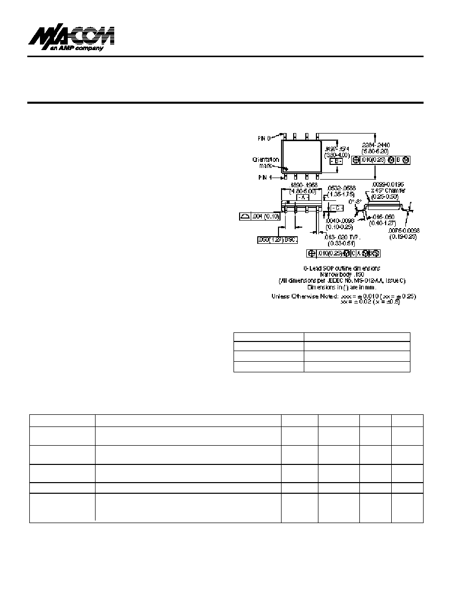
S O - 8
1. All measurements at 1 GHz in a 50-
system, unless otherwise specified.The RF ports must be blocked outside of the package
from ground or any other voltage.
q
q
q
q
q
q
q
O rdering Info r m a t i o n
Electrical Specifications
1
, TA = +25∞C
*
If specific reel size is required, consult factory for part number
assignment.
V 2.00
Voltage Variable Absorptive Attenuator, 35 dB
AT-109
Absolute Maximum Ratings
1
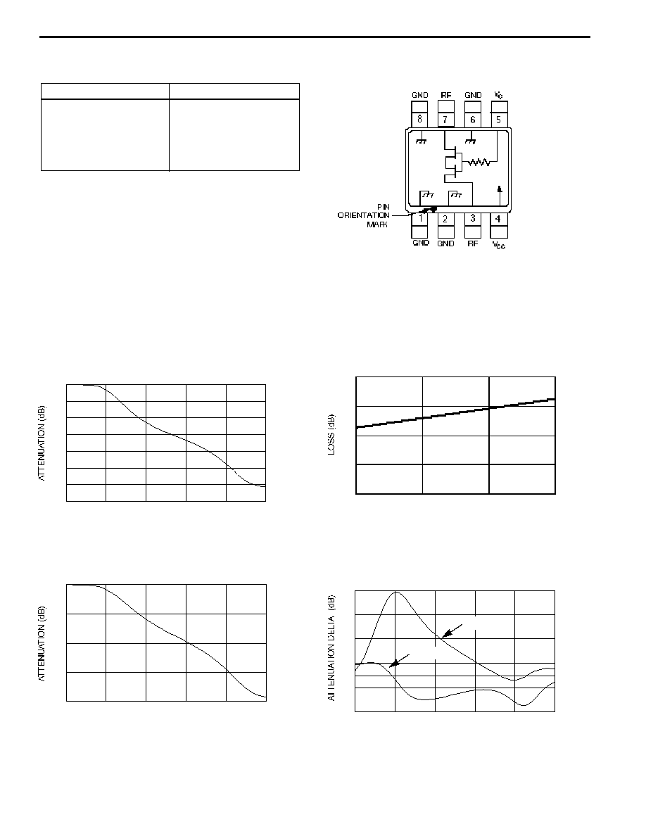
Functional Sch e m a t i c
1. Operation of this device above any one of these parameters may
cause permanent damage.
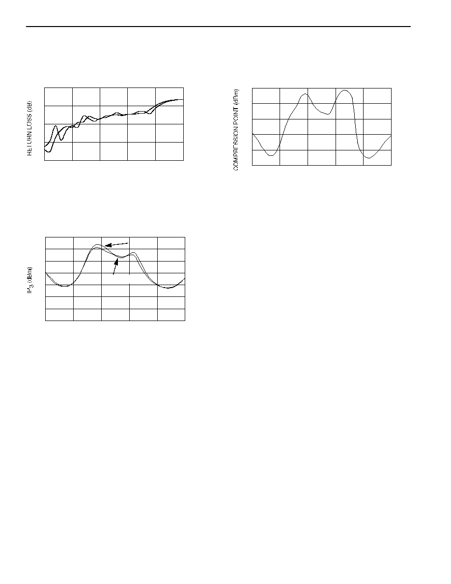
Typical Performance
VCC = +5 VDC ±0.5 VDC @ 50 µA max.
VC = 0 VDC to +5 VDC @ 50 µA max.
External DC blocking capacitors are required on all RF ports.
Parameter
Absolute Maximum
Maximum Input Power
+21 dBm
Supply Voltage VCC
-1 V, +8 V
Control Voltage VCC
-1 V, VCC + 0.5 V
Operating Temperature
-40∞C to +85∞C
Storage Temperature
-65∞C to +150∞C
ATTENUATION
vs
CONTROL VOLTAGE
@ +25∞C, F = 1800 MHz
0
-5
-10
-15
-20
-25
-30
-35
5
4
3
2
1
0
CONTROL VOLTAGE (VOLTS)
RELATIVE ATTENUATION
vs
CONTROL VOLTAGE
@ +25∞C, F = 900 MHz
0
-10
-20
-30
-40
5
4
3
2
1
0
CONTROL VOLTAGE (VOLTS)
INSERTION LOSS
vs
FREQUENCY
4.0
3.0
2.0
1.0
0
0.5
1.0
1.5
2.0
FREQUENCY (GHz)
ATTENUATION
vs
TEMPERATURE,
NORMALIZED TO +25∞C, F = 900 MHz
3.5
2.5
1.5
0.5
-0.5
-1.5
5
4
3
2
1
0
CONTROL VOLTAGE (VOLTS)
-40∞C
+85∞C