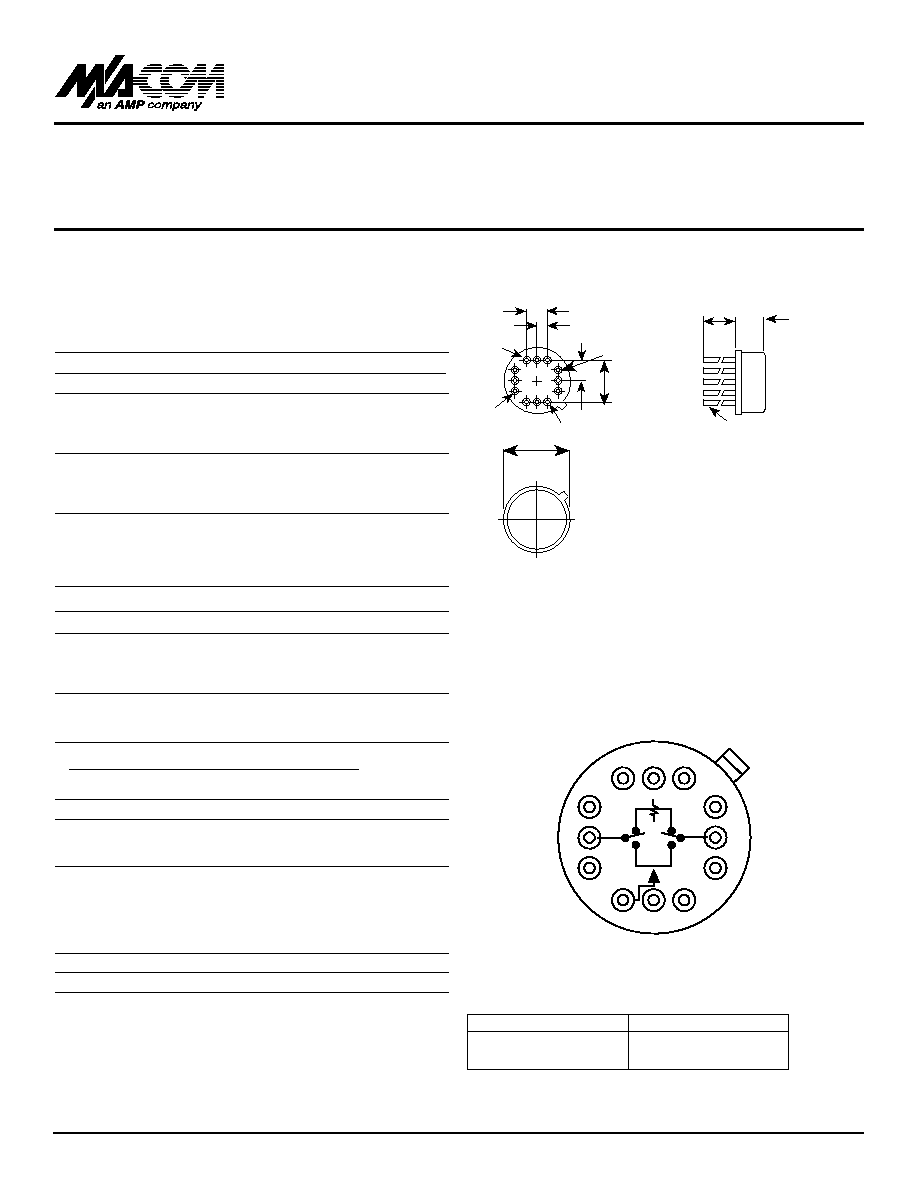
0.100 TYP (2.54)
0.200 TYP (5.08)
0.250 MIN
(6.35) 0.187 MAX
(4.75)
0.018
±
0.005
PIN DIA
(0.46
±
0.13)
0.60 DIA
(15.2 )
0.200 TYP (5.08)
P7
P4
P10
0.400 (10.16)
TYP
P1
Bottom of Case is AC Ground
Dimensions in ( ) are in mm.
Unless Otherwise Noted: .xxx = ± 0.010 (.xx = ± 0.25)
.xx = ± 0.02 (.x = ±0.5)
1 Bit, 10 dB, GaAs Digital Atten uator
0.02 - 2 GHz
AT-358
T0-8-2
Functional Sc hematic (T op Vie w)
C1 State
0 Reference Loss
1 Attenuation
T ruth T a b l e
Guaranteed Specifications
1
(From -55∞C to +85∞C)
Frequency Range 0.02 ≠ 2.0 GHz
Nominal Attenuation
2
10 dB
Attenuation Accuracy 0.02 ≠ 2.0 GHz +/-0.5 dB Max
0.02 ≠ 1.0 GHz +/-0.3 dB Max
0.02 ≠ 0.5 GHz +/-0.2 dB Max
0.02 ≠ 0.2 GHz +/-0.2 dB Max
VSWR 0.02 ≠ 2.0 GHz 1.9:1 Max
0.02 ≠ 1.0 GHz 1.3:1 Max
0.02 ≠ 0.5 GHz 1.3:1 Max
0.02 ≠ 0.2 GHz 1.3:1 Max
Reference Insertion Loss
0.02 ≠ 2.0 GHz 2.7 dB Max
0.02 ≠ 1.0 GHz 1.0 dB Max
0.02 ≠ 0.5 GHz 0.9 dB Max
0.02 ≠ 0.2 GHz 0.8 dB Max
Operating Characteristics
Impedance 50 Ohms Nominal
Switching Characteristics
Ton, Toff (50% CTL to 90%/10% RF) 100 ns Typ
Trise, Tfall (10%/90% or 90%/10% RF) 40 ns Typ
Switching Transients (Unfiltered) 50 mV Typ
Input Power for 1 dB Compression
0.5 ≠ 2.0 GHz +24 dBm Typ
0.05 GHz +18 dBm Typ
Intermodulation Intercept Point (for two-tone input power up to +5 dBm)
Intercept Points IP2 IP3
0.5 ≠ 2.0 GHz +58 +38 dBm Typ
0.05 GHz +54 +35 dBm Typ
Bias Power +5 VDC @ 1 mA Max
Control Voltages
Vin Low (0) 0.0 to 1.5V @ 1µA Max
Vin High (1) 3.5 to 5.0V @ 1µA Max
1. All specifications apply with 50 ohm impedance connected to all RF ports, with +5
VDC bias voltage.
2. Above reference insertion loss.
3. Contact the factoy for standard or custom screening requirements.
Or dering Inf ormation
Model No. Package
AT-358 PIN TO-8-2
Features
∑
CMOS Control Interface
∑
Low Power Consumption
GND
GND
+5V
GND
GND
RF IN
RF OUT
10 dB
GND
GND
GND
GND
CI
Specifications Subject to Change Without Notice. V2.01
Parameter Absolute Maximum
1
Max. Input Power
0.05 GHz +27 dBm
0.5 ≠ 2.0 GHz +32 dBm
Bias Voltage 0.5 to +7 V
Control Voltage -0.5 to V bias + 0.5 V
Operating Temperature ≠55∞C to +125∞C
Storage Temperature ≠65∞C to +150∞C
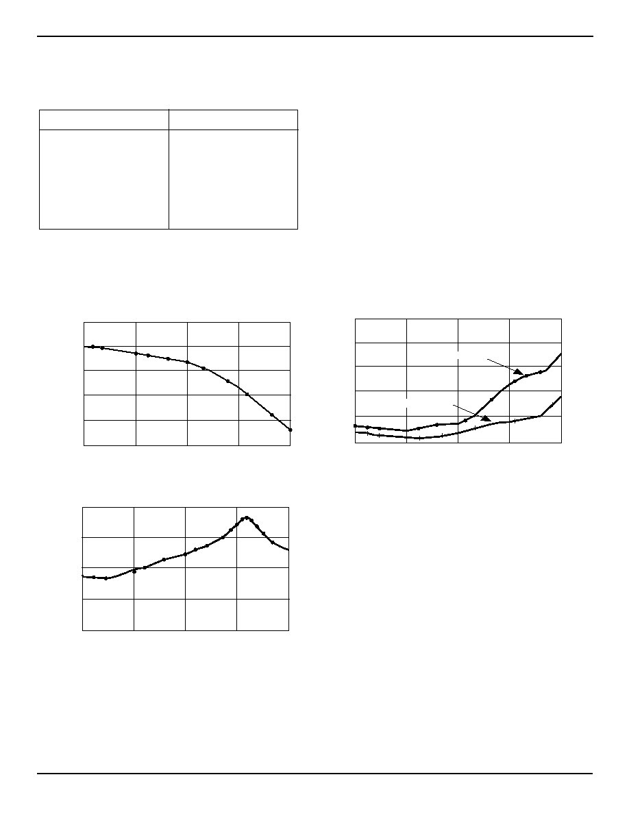
Typical Performance
1. Operation of this device above any one of these parameters may
cause permanent damage.
Absolute Maximum Ratings
0
-0.5
-1.0
-1.5
-2.0
-2.5
FREQUENCY (GHz)
LOSS (dB)
REFERENCE INSERTION LOSS vs FREQUENCY
0.5
0.02 1.0 1.5 2.0
FREQUENCY (GHz)
DEVIATION FROM
NOMINAL ATTENUATION (dB)
ATTENUATION FLATNESS vs FREQUENCY
0.02 0.5 1.0 1.5 2.0
-0.5
-0.25
0
+0.25
+0.5
ATTENUATION STATE
LOSS STATE
1.4
1.2
VSWR
VSWR vs FREQUENCY
2.0
1.8
1.6
1.0
FREQUENCY (GHz)
0.5
0.02 1.0 1.5 2.0
Specifications Subject to Change Without Notice. V2.01
1-Bit, 10 dB, GaAs Digital Attenuator AT-358