Low Cost SMT Dual Band Diplexer
DP52-0002
M/A-COM Division of AMP Incorporated
s
North America: Tel. (800) 366-2266, Fax (800) 618-8883
s
Asia/Pacific: Tel.+85 2 2111 8088, Fax +85 2 2111 8087
s
Europe: Tel. +44 (1344) 869 595, Fax+44 (1344) 300 020
www.macom.com
AMP and Connecting at a Higher Level are trademarks.
Specifications subject to change without notice.
V2.00
Features
∑
Small Size and Low Profile
∑
Industry Standard SOIC-8 SMT Plastic Package
∑
Superior Repeatability
∑
Passbands 824 - 960 MHz and 1850 - 1990 MHz
∑
Passbands 880 - 960 MHz and 1700 - 1900 MHz
∑
Typical Passband Insertion Loss: 0.5 dB
∑
2 Watt Power Handling
∑
Low Cost
Description
M/A-COM's DP52-0002 is an IC-based monolithic diplexer in a
low cost SOIC-8 SMT plastic package. This diplexer is ideally
suited for applications where small size, low insertion loss, supe-
rior repeatability and low cost are required. Typical applications
include AMPS/PCS and GSM/DCS dual mode portable devices.
The DP52-0002 is fabricated using a passive-integrated circuit
process. The process features full-chip passivation for increased
performance and reliability.
SO-8
1. If specific reel size is required, consult factory for part number
assignment.
Part Number
Package
DP52-0002
DP52-0002-TR
SOIC-8-Lead Plastic Package
Forward Tape and Reel
1
1. All specifications apply with a 50-ohm source and load impedance.
824 - 960 / 1850 - 1990 MHz Typical Electrical Specifications
1
, T
A
= +25∫C
Parameters
Units
Min.
Typ.
Max.
Passband Insertion Loss
dB
--
0.5
0.8
Stopband Isolation
dB
12
18
--
Passband VSWR
--
--
1.4:1
1.7:1
Ordering Information
Low Cost SMT Dual Band Diplexer
824 ≠ 960 / 1850 ≠ 1990 MHz (AMPS/PCS)
880 ≠ 960 / 1700 ≠ 1900 MHz (GSM/DCS)
DP52-0002
1. All specifications apply with a 50-ohm source and load impedance.
880 - 960 / 1700 - 1900 MHz Typical Electrical Specifications
1
, T
A
= +25∫C
Parameters
Units
Min.
Typ.
Max.
Passband Insertion Loss
dB
--
0.5
0.9
Stopband Isolation
dB
12
18
--
Passband VSWR
--
--
1.5:1
1.8:1
0∞-8∞
.0075-0.0098
(0.19-0.25)
.1890-.1968
(4.80-5.00)
.0099-0.0196
x 45∞ Chamfer
(0.25-0.50)
.2284-.2440
(5.80-6.20)
PIN 8
Orientation
mark
PIN 1
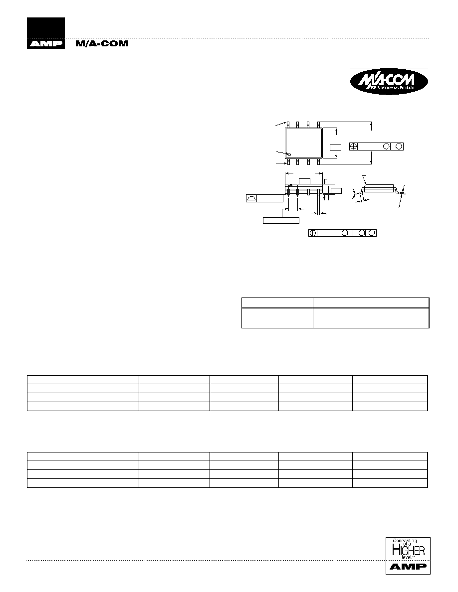
8- Lead SOP outline dimensions
Narrow body .150
(All dimensions per JEDEC No. MS-012-AA, Issue C)
Dimensions in ( ) are in mm.
.1497-.1574
(3.80-4.00)
- B -
- A -
.050(1.27) BSC.
.013-.020 TYP.
(0.33-0.51)
.0040-.0098
(0.10-0.25)
- C -
.0532-.0688
(1.35-1.75)
.016-.050
(0.40-1.27)
.010(0.25) M B M
.010(0.25) M C A M B S
Unless Otherwise Noted: .xxx = ± 0.010 (.xx = ± 0.25)
.xx = ± 0.02 (.x = ±0.5)
.004 (0.10)

Low Cost SMT Dual Band Diplexer
DP52-0002
M/A-COM Division of AMP Incorporated
s
North America: Tel. (800) 366-2266, Fax (800) 618-8883
s
Asia/Pacific: Tel.+85 2 2111 8088, Fax +85 2 2111 8087
s
Europe: Tel. +44 (1344) 869 595, Fax+44 (1344) 300 020
www.macom.com
AMP and Connecting at a Higher Level are trademarks.
Specifications subject to change without notice.
V2.00
Absolute Maximum Ratings
1
Parameter
Absolute Maximum
Input Power
Operating Temperature
Storage Temperature
2W CW
-40∞C to +85∞C
-65∞C to 150∞C
1. Exceeding these limits may cause permanent damage.
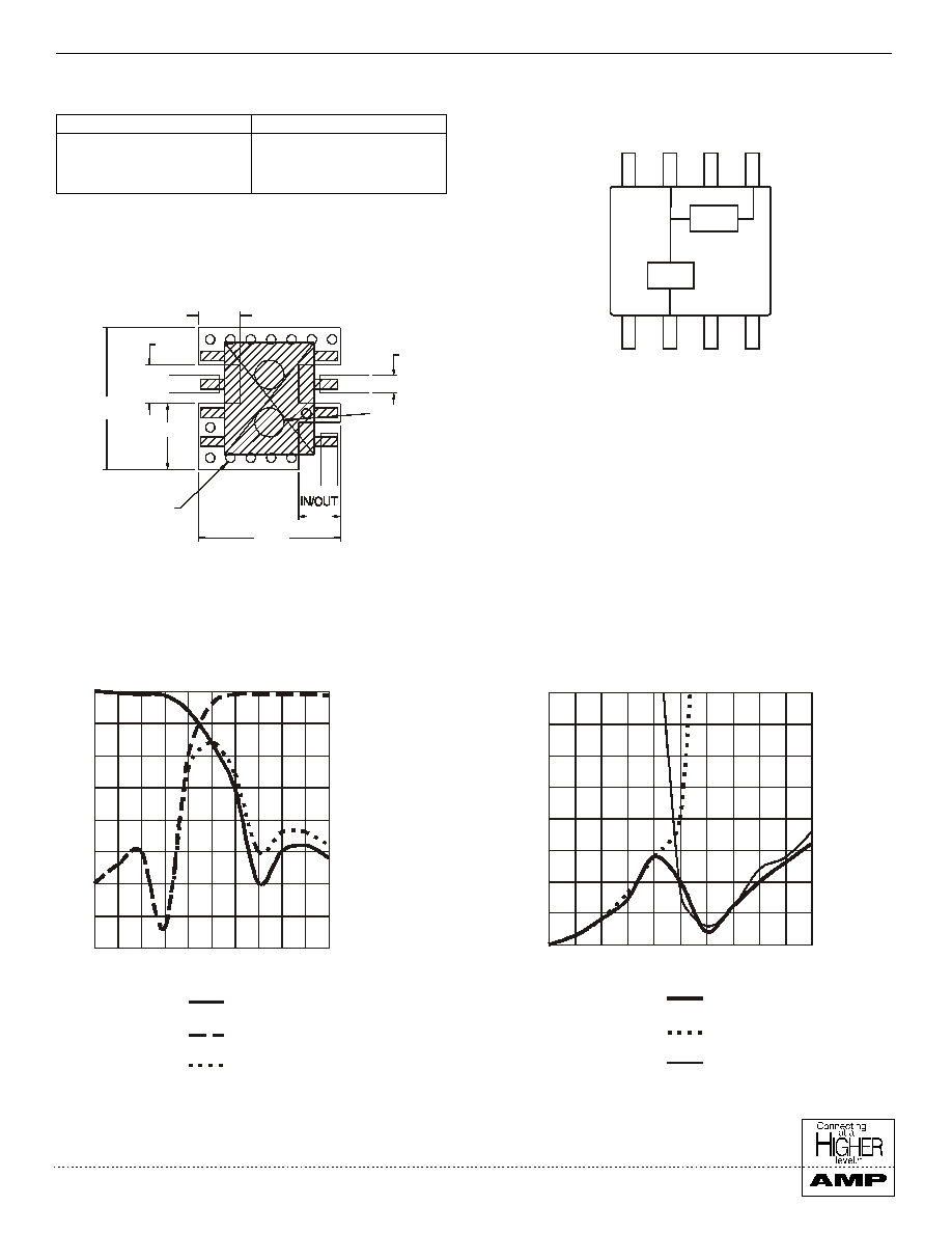
Functional Diagram
Typical Performance @ +25∞C
VSWR vs. Frequency
Insertion Loss vs. Frequency
Recommended PCB Configuration
P C S
.0 50 P L AT E D
T H R U (2 X )
.
0 16 P L AT E D
T H RU (1 4 X )
A M P S IN /O U T
A N T E N N A
.0 30 T Y P.
.2 44
.0 72
.0 72
.2 44
.11 3
.0 67
T Y P.
C IR C U IT M AT E R IA L : F R -4, .0 16 T H IC K .
HPF
LPF
1
8
4
5
AMPS
IN/OUT
ANTENNA
GND
GND
PCS
IN/OUT
GND
GND
GND
A ll u nu s ed pins m us t be R F an d D C gro u nd ed .
P ins 1 an d 4 a re th erm a l g rou nd c on ta cts.
IN
SER
T
ION
LOSS dB
VSW
R
0
-5
-10
-15
-20
-25
-30
-35
-40
3
2.75
2.5
2.25
2
1.75
1.5
1.25
1
0
300 600 900
1200 1500 1800 2100 2400 2700 3000
Antenna /
AMPS, GSM
Antenna /
PCS, DCS
AMPS / PCS
GSM/DCS
Antenna
AMPS, GSM
PCS, DCS
FREQUENCY MHz
0
300
600 900
1200 1500 1800
2100 2400 2700
3000
FREQUENCY MHz

