SPDT PIN Diode Driver
DR65
-
0003
SO-8
V 5.00
Features
n
Moderate Speed, CMOS Technology (25 nS)
n
Complementary Outputs
n
High Drive Current Capability (± 50 mA)
n
Low Current Consumption
n
Plastic SOIC Body for SMT Applications
n
Tape and Reel Packaging Available
Description
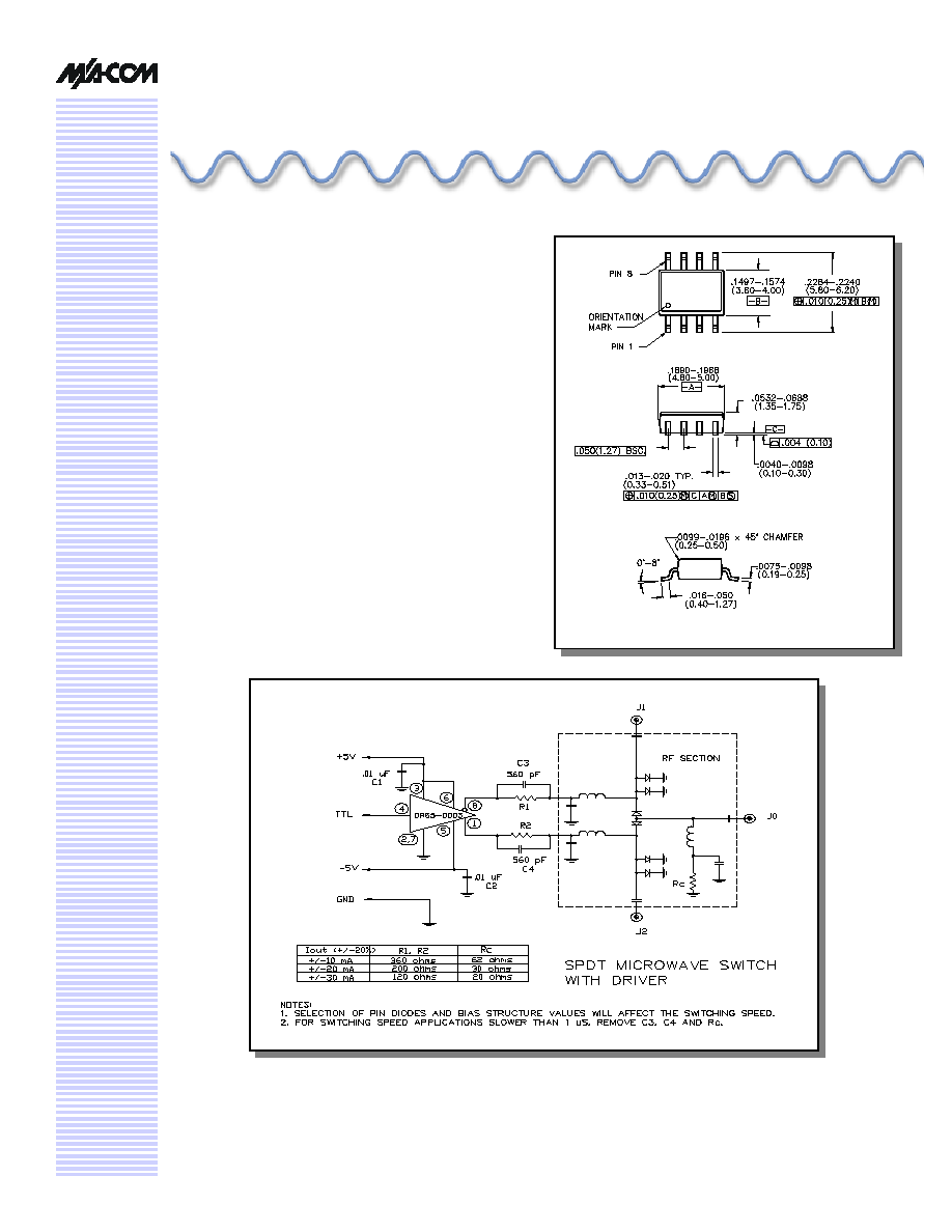
M/A-COM's DR65-0003 is a SPDT driver used to interface
between TTL logic signals and PIN diode based microwave
switches. High-speed analog CMOS technology is used to
achieve low power consumption at moderate speeds. Low
output resistances allow it to develop high output current
spikes to ensure fast switching speeds. The complementary
output stages are structured so it can be used as an inverting
or non-inverting driver for SPST switches, or as a single
input, complementary driver for SPDT switches. The
monolithic die is packaged in a SO-8, plastic surface mount
package and is available in tape and reel packaging for high
volume applications. The DR65-0003 is ideally suited for
driving M/A-COM's line of HMIC switches.
Package outline conforms to JEDEC standard MS-012AA.

SPDT PIN Diode Driver
DR65-0003
Specifications subject to change without notice.
n
North America: Tel. (800) 366-2266
n
Asia/Pacific: Tel.+81-44-844-8296, Fax +81-44-844-8298
n
Europe: Tel. +44 (1344) 869 595, Fax+44 (1344) 300 020
Visit www.macom.com for additional data sheets and product information.
V 5.00
2
Electrical Specifications, T
A
= +25
∞
C, +Vcc = + Vdd = + 5.0V ± 5%,
-Vee = - 5.0V ±5%
Parameter
Test Conditions
Units
Min
Typical
Max
Switching Speed
1
Delay
Rt/Ft
Spike current into 10 ohm load
50 % TTL to 90%
10%-90%; 90%-10%
nS
nS
--
--
25
2
35
5
PRF
50% duty cycle
MHz
DC
--
5
Output Voltage Drop, No Load
With reference to supply voltage
V
--
--
.25
DC Output Current
Peak Spike Output Current
Load Dependant
Spiking Capacitor in Circuit
mA
mA
--
--
±30
±150
±50
±200
Output Stage on Resistance
Positive Output FET, Qp
Negative Output FET, Qn
--
--
15
20
20
25
Quiescent Supply Currents
+5V
-5V
mA
mA
--
--
--
--
1.0
.2
TTL Levels
Logic "0" @ 20 µA sink current
Logic "1" @ 20 µA source current
V
V
0
2.0
--
--
.8
5.0
Package Dissipation
--
mW
--
--
200
1. Decoupling capacitors (.01 µF) are required on power supply lines.
Absolute Maximum Ratings
2
Parameter
Absolute Maximum
+V
CC
5.5V
+Vdd must be = or < +Vcc
+Vcc
+Vee
-5.5V
TTL Input Voltage
-0.5 V to Vcc +0.5V
Operating Temperature
-40∫C to +85∫C
Storage Temperature
-65∫C to +125∫C
2. Operation of this device above any one of these parameters
may cause permanent damage.
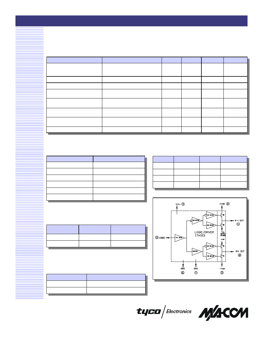
Pin Function Table
Pin #
Function
Pin #
Function
1
N-I OUT
5
+Vee
2
GND
6
+Vdd
3
+Vcc
7
GND
4
LOGIC
8
INV OUT
Part Number
Package
DR65-0003
Bulk Packaging
DR65-0003TR
Tape & Reel (1K Reel)
Ordering Information
Truth Table
Logic Input
(Pin 4)
N-I Out (Pin 1)
INV Out (Pin 8)
"0"
L
H
"1"
H
L
H: Iout is +Current
L: Iout is -Current

