 | –≠–ª–µ–∫—Ç—Ä–æ–Ω–Ω—ã–π –∫–æ–º–ø–æ–Ω–µ–Ω—Ç: DR65-0008 | –°–∫–∞—á–∞—Ç—å:  PDF PDF  ZIP ZIP |
Quad Positive Voltage Driver for GaAs FET
Switches and Attenuators
DR65
-
0008
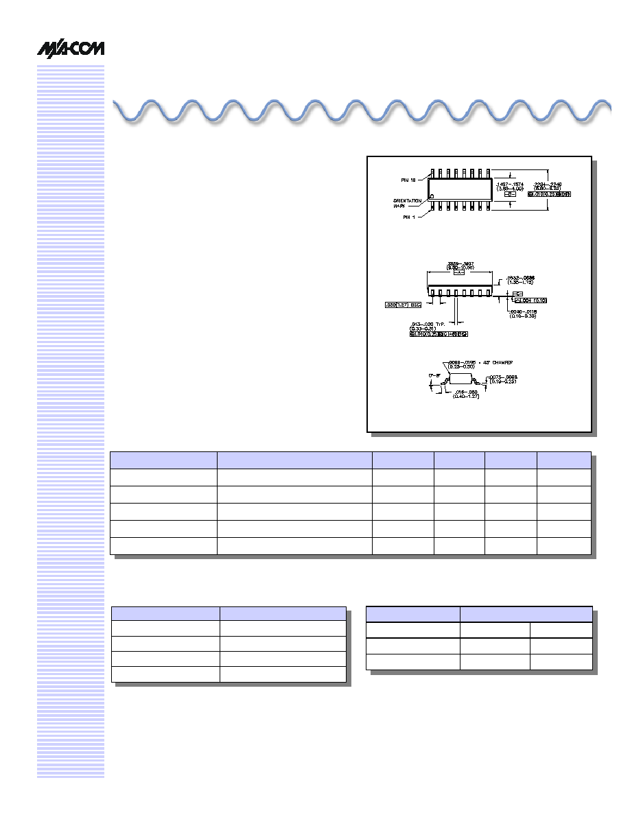
SO-16
V 2.00
Features
n
High Speed CMOS Technology
n
Complementary Positive Voltage Outputs for driving
series and shunt FETS
n
TTL Inputs
n
Low Power Dissipation
n
Plastic SOIC Package for SMT Applications
n
Tape and Reel Packaging Available
n
Low Output Impedance for Driving Capacitive Circuits
Description
M/A-COM's DR65-0008 is a Quad channel driver used
to translate TTL control inputs into gate voltages for
Positive Voltage, GaAs FET microwave switches and
attenuators. High speed analog CMOS technology is
utilized to achieve low power dissipation at moderate to
high speeds, encompassing most microwave switching
applications.
Package outline conforms to JEDEC standard MS-012AC
Guaranteed Operating Ranges
Parameter
Test Conditions
1
Units
Min
Typ
Max
V
CC
Positive DC Supply Voltage
V
4.5
5.0
5.5
T
A
Operating Ambient Temperature
∞C
-40
+25
+85
I
OH
DC Output Current - Source
mA
30
--
--
I
OL
DC Output Current - Sink
mA
-30
--
--
Trise, Tfall
Maximum Input Rise or Fall Time
nS
--
--
500
1. All voltages are relative to GND
Absolute Maximum Ratings
Parameter
Absolute Maximum
V
CC
- .5V to + 6.0 V
V
IN
2
- .5V to V
CC
+ .5 V
V
OUT
0.0V to Vcc
Storage Temperature
-65∞C to +150∞C
Truth Table
Input
C
X
A
X
B
X
0
GND
V
CC
1
V
CC
GND
Outputs
2. Standard CMOS TTL interface, latch-up will occur if logic
signal is applied prior to power supply.
Quad Positive Voltage Driver for GaAs FET Switches and Attenuators
DR65-0008
Specifications subject to change without notice.
n
North America: Tel. (800) 366-2266
n
Asia/Pacific: Tel.+81-44-844-8296, Fax +81-44-844-8298
n
Europe: Tel. +44 (1344) 869 595, Fax+44 (1344) 300 020
Visit www.macom.com for additional data sheets and product information.
V 2.00
2
PIN
Function
PIN
Function
1
A3
9
C2
2
B3
10
C1
3
A4
11
V
CC
4
B4
12
GND
5
GND
13
A1
6
V
CC
14
B1
7
C4
15
A2
8
C3
16
B2
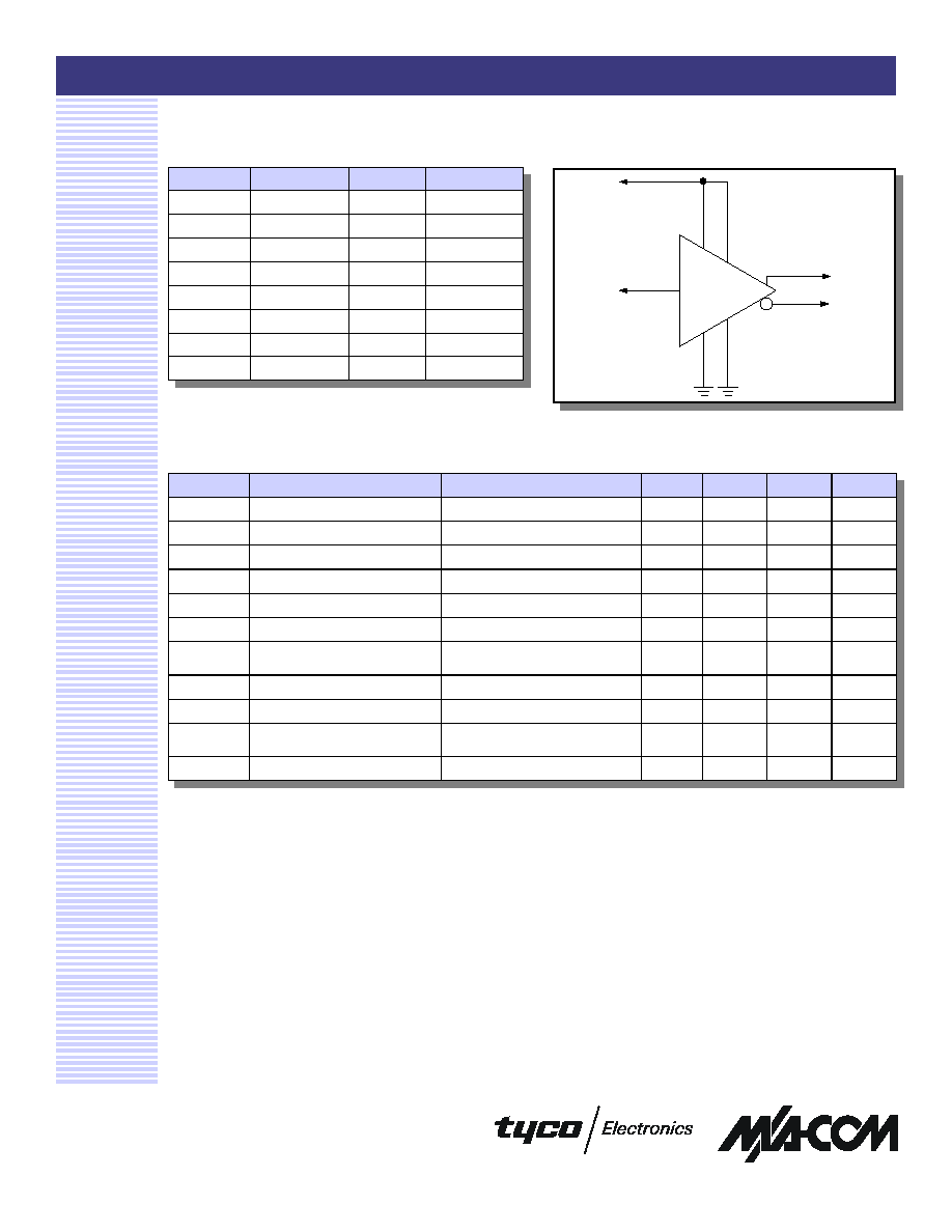
Pin Configuration
Logic Diagram
Vcc
Cx
Ax
Bx
AC & DC Characteristics Over Guaranteed Operating Range
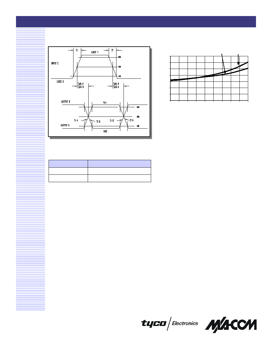
See Switching Wave Forms for the definition of the switching terms.
Vcc must be by-passed with .01 µF Capacitors.
Unused inputs must be tied to Ground
Symbol
Parameter
Test Conditions
Units
Min
Typ
Max
V
IH
Input HIGH Voltage
Guaranteed HIGH Input Voltage
V
2.0
--
--
V
IL
Input LOW Voltage
Guaranteed LOW Input Voltage
V
--
--
0.8
V
OH
Output HIGH Voltage
I
OH
= 1 mA
V
V
CC
- 0.1
--
--
I
IN
Input Leakage Current
V
IN
= V
CC
or GND
µA
-10.0
0
+10.0
I
CC
Quiescent Supply Current
V
CC
= Max
µA
--
--
400
I
CC
Additional Supply Current, per
TTL Input pin
V
CC
= Max
mA
--
--
1.0
T
PHL,
T
PLH
Propagation Delay
Guaranteed -40∞ C to + 85∞ C
nS
--
30
50
T
THL,
T
TLH
Output Transition Time
Guaranteed -40∞ C to + 85∞ C
nS
--
10
25
T
SKEW
Delay Skew,
Output A to Output B
Guaranteed -40∞ C to + 85∞ C
nS
--
--
8
R
out
Output Resistance
I
O
= ± 30 mA
O
--
40
--
V
OL
Output LOW Voltage
I
OL
= -1 mA
V
--
--
.1
Quad Positive Voltage Driver for GaAs FET Switches and Attenuators
DR65-0008
Specifications subject to change without notice.
n
North America: Tel. (800) 366-2266
n
Asia/Pacific: Tel.+81-44-844-8296, Fax +81-44-844-8298
n
Europe: Tel. +44 (1344) 869 595, Fax+44 (1344) 300 020
Visit www.macom.com for additional data sheets and product information.
V 2.00
Output Impedance vs. Output Current
3
Part Number
Package
DR65-0008
Bulk Packaging
DR65-0008-TR
Tape & Reel (1K Reel)
Ordering Information
Switching Waveforms
0
10
20
30
40
50
60
70
5
10
15
20
25
30
35
40
45
50
Output Current (± mA)
Output Resistance (W)
Source
Sink