Äîêóìåíòàöèÿ è îïèñàíèÿ www.docs.chipfind.ru
Specifications subject to change without notice.
n
North America: Tel. (800) 366-2266
n
Asia/Pacific: Tel.+81-44-844-8296, Fax +81-44-844-8298
n
Europe: Tel. +44 (1344) 869 595, Fax+44 (1344) 300 020
1
Visit www.macom.com for additional data sheets and product information.
3.6 V, 450 mW DECT RF Power
Amplifier IC
V 1.0
Features
§
Ideal for DECT Applications
§
+26.5 dBm Output Power
§
24.5 dB Power Gain
§
Single Positive Supply
§
Class A Bias
§
No External RF Matching Required
Description
The MA02203AD is a two stage power amplifier
designed for DECT applications to have an output
power of +26.5 dBm with an input power of 2 dBm.
This power amplifier operates at +3.6 volts with
35% typical power added efficiency. The
MA02203AD is mounted in a narrow body 16-pin
SOIC plastic package.
The MA02203AD is fabricated using M/A-COM's
self-aligned MSAG
®
-Lite MESFET process for a low
single supply voltage, high power efficiency, and
excellent reliability.
This part is
not
recommended for new designs. M/A-
COM's MA02206GJ has superior RF performance
with less DC power consumption in a smaller
package. Pricing on the MA02206GJ is also less
than the MA02203AD.
Ordering Information
Part Number
Description
MA02203AD-R7
7 inch, 1000 piece reel
MA02203AD-R13
13 inch, 3000 piece reel
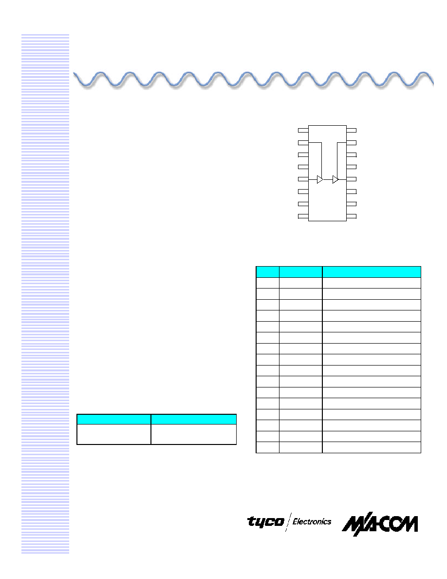
Functional Schematic
GND
GND
RF
IN
GND
GND
N/C
GND
GND
RF
OUT
GND
GND
+V
DD1
N/C
+V
DD2
N/C
N/C
16 pin narrow body SOIC
Pin Configuration
Pin
Function
Description
1
N/C
Not Connected
2
V
DD1
First Stage Supply Voltage
3
GND
Ground
4
GND
Ground
5
RF
IN
RF Input
6
GND
Ground
7
GND
Ground
8
N/C
Not Connected
9
N/C
Not Connected
10
GND
Ground
11
GND
Ground
12
RF
OUT
RF Output
13
GND
Ground
14
GND
Ground
15
V
DD2
Second Stage Supply Voltage
16
N/C
Not Connected
MA02203AD
Part Description
Specifications subject to change without notice.
n
North America: Tel. (800) 366-2266
n
Asia/Pacific: Tel.+81-44-844-8296, Fax +81-44-844-8298
n
Europe: Tel. +44 (1344) 869 595, Fax+44 (1344) 300 020
2
Visit www.macom.com for additional data sheets and product information.
3.6 V, 450 mW DECT RF Power Amplifier IC
MA02203AD
V 1.0
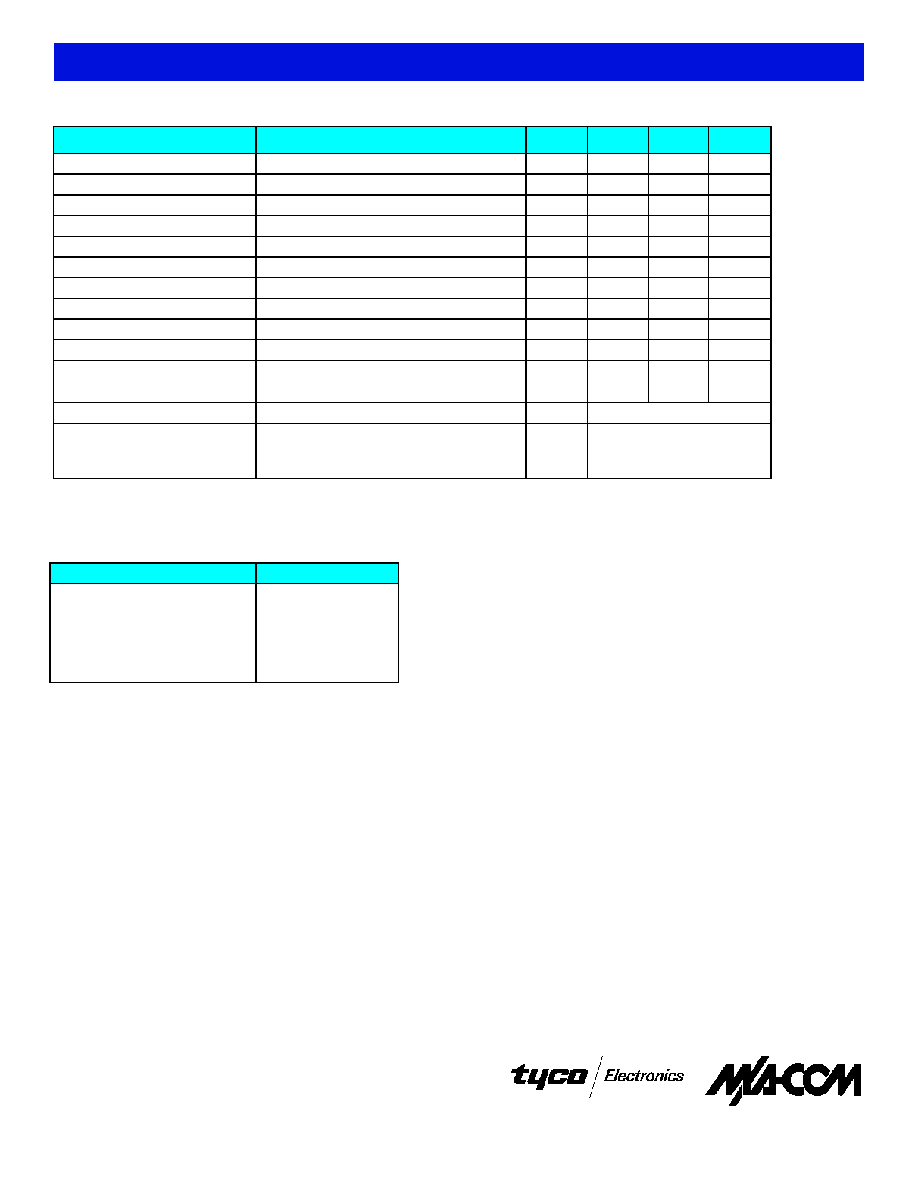
Electrical Specifications: T
S
= 40 °C
1
, Z
0
= 50
2,3
Parameter
Test Conditions
Units
Min
Typ
Max
Frequency
MHz
1880
1900
Output Power
dBm
25.5
26.5
27.5
Pout Frequency Dependency
dB
0.2
0.5
Power Gain
dB
24.5
Current Consumption
mA
350
420
Input VSWR, PA On
-
1.6:1
2.0:1
Input VSWR, PA Off
V
DD1
, V
DD2
= 0 V
-
1.4:1
2.0:1
Isolation, PA Off
V
DD1
, V
DD2
= 0 V
dB
40
2
nd
Harmonics
dBc
31
3
rd
Harmonics
dBc
55
Thermal Resistance
Junction of 2nd stage FET to pin 11, Duty
Cycle=50%
o
C/W
63
Load Mismatch
V
DD
= 4.6 V, VSWR = 10:1, P
IN
= 7 dBm
-
No degradation
Stability
P
IN
= -3 to +7 dBm, V
DD
= 0 - 4.6 V, 0 mW
< P
OUT
< 450 mW, T
S
= -40 to +75
°
C, Load
VSWR = 10:1
-
All spurs < -60 dBc
1. Ts is the temperature measured at the soldering point of pin 11.
2. Unless otherwise specified, input power is +2 dBm, V
DD
is +3.6 V, and test frequency is 1890 MHz.
Absolute Maximum Ratings
1
Parameter
Absolute Maximum
Max Input Power
+6 dBm
Operating Voltages
+5.5 volts
Operating Temperature, Ts
-40 °C to +75 °C
Channel Temperature
+150 °C
Storage Temperature
-40 °C to +150 °C
1. Exceeding any one or combination of these limits may cause permanent damage.
Part Description
Specifications subject to change without notice.
n
North America: Tel. (800) 366-2266
n
Asia/Pacific: Tel.+81-44-844-8296, Fax +81-44-844-8298
n
Europe: Tel. +44 (1344) 869 595, Fax+44 (1344) 300 020
3
Visit www.macom.com for additional data sheets and product information.
3.6 V, 450 mW DECT RF Power Amplifier IC
MA02203AD
V 1.0
Application Information
Static Sensitivity
Gallium arsenide integrated circuits are ESD sensitive and can be damaged by static electricity. Use proper ESD precautions when
handling these devices.
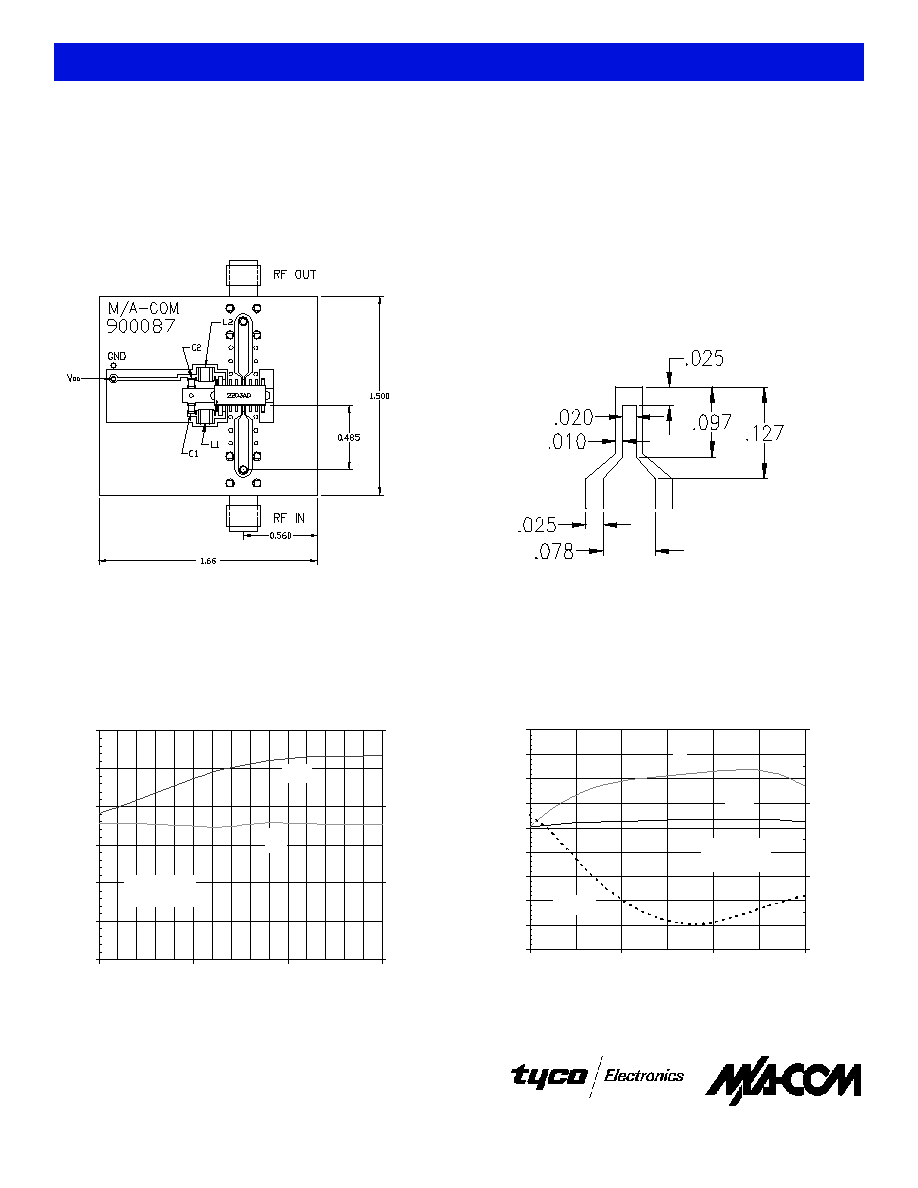
Board Layout
Sample Test Board
50 Ohm Lead Transition
Typical Performance Curves
Output Power and Current vs. Input Power
0
5
10
15
20
25
30
-10
-5
0
5
P
IN
, Input Power (dBm)
P
OUT
, Output Power (dBm)
0.0
0.2
0.4
0.6
I
DD
, Drain Current (A)
P
OUT
I
DD
f = 1.89 GHz
V
DD
= 3.6 V
Output Power, PAE, and VSWR vs. Frequency
0
5
10
15
20
25
30
35
40
45
1.7
1.8
1.9
2
, Frequency (GHz)
P
OUT
(dBm) and
(%)
1:1
2:1
3:1
4:1
Input VSWR
P
OUT
P
IN
= +2 dBm
V
DD
= 3.6 V
VSWR
Part Description
Specifications subject to change without notice.
n
North America: Tel. (800) 366-2266
n
Asia/Pacific: Tel.+81-44-844-8296, Fax +81-44-844-8298
n
Europe: Tel. +44 (1344) 869 595, Fax+44 (1344) 300 020
4
Visit www.macom.com for additional data sheets and product information.
3.6 V, 450 mW DECT RF Power Amplifier IC
MA02203AD
V 1.0
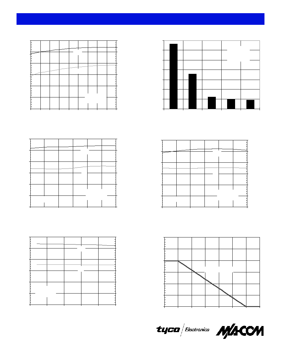
Output Power and Current vs. Supply Voltage
0
5
10
15
20
25
30
2.8
3.0
3.2
3.4
3.6
3.8
4.0
4.2
4.4
4.6
V
DD
, Supply Voltage (V)
P
OUT
, Output Power (dBm)
0
0.1
0.2
0.3
0.4
0.5
0.6
I
DD
, Drain Current (A)
=1.89 GHz
P
IN
= +2 dBm
P
OUT
I
DD
Output Power and Current vs. Frequency, Ts = -40
o
C
0
5
10
15
20
25
30
1.7
1.8
1.9
2
, Frequency (GHz)
P
OUT
, Ouput Power (dBm)
0
0.1
0.2
0.3
0.4
0.5
0.6
I
DD
, Drain Current (A)
P
OUT
I
DD
P
IN
= +2 dBm
V
DD
= 3.6 V
T
s
= -40 °C
Output Power and Current vs. Temperature
0
5
10
15
20
25
30
-50
-25
0
25
50
75
T
S
, Operating Temperature (°C)
P
OUT
, Output Power (dBm)
0.0
0.1
0.2
0.3
0.4
0.5
0.6
I
DD
, Drain Current (A)
I
DD
P
OUT
P
IN
= +2 dBm
V
DD
= 3.6 V
Harmonics
-40
-30
-20
-10
0
10
20
30
2
3
4
5
Frequency
P
OUT
, Output Power (dBm)
o
= 1.89 GHz
P
IN
= +2 dBm
V
DD
= 3.6 V
Output Power and Current vs. Frequency, Ts = +75
o
C
0
5
10
15
20
25
30
1.7
1.8
1.9
2
, Frequency (GHz)
P
OUT
, Ouput Power (dBm)
0
0.1
0.2
0.3
0.4
0.5
0.6
I
DD
, Drain Current (A)
P
OUT
I
DD
P
IN
= +2 dBm
V
DD
= 3.6 V
T
s
= +75 °C
Power Dissipation vs. Temperature
0.0
0.5
1.0
1.5
2.0
2.5
3.0
0
25
50
75
100
125
150
175
T
S
, Temperature at Solder Point of Pin 11 (°C)
P
DISS
, Dissipated Power (W)
Slope = -1 / R
TH J-S
Part Description
Specifications subject to change without notice.
n
North America: Tel. (800) 366-2266
n
Asia/Pacific: Tel.+81-44-844-8296, Fax +81-44-844-8298
n
Europe: Tel. +44 (1344) 869 595, Fax+44 (1344) 300 020
5
3.6 V, 450 mW DECT RF Power Amplifier IC
MA02203AD
V 1.0
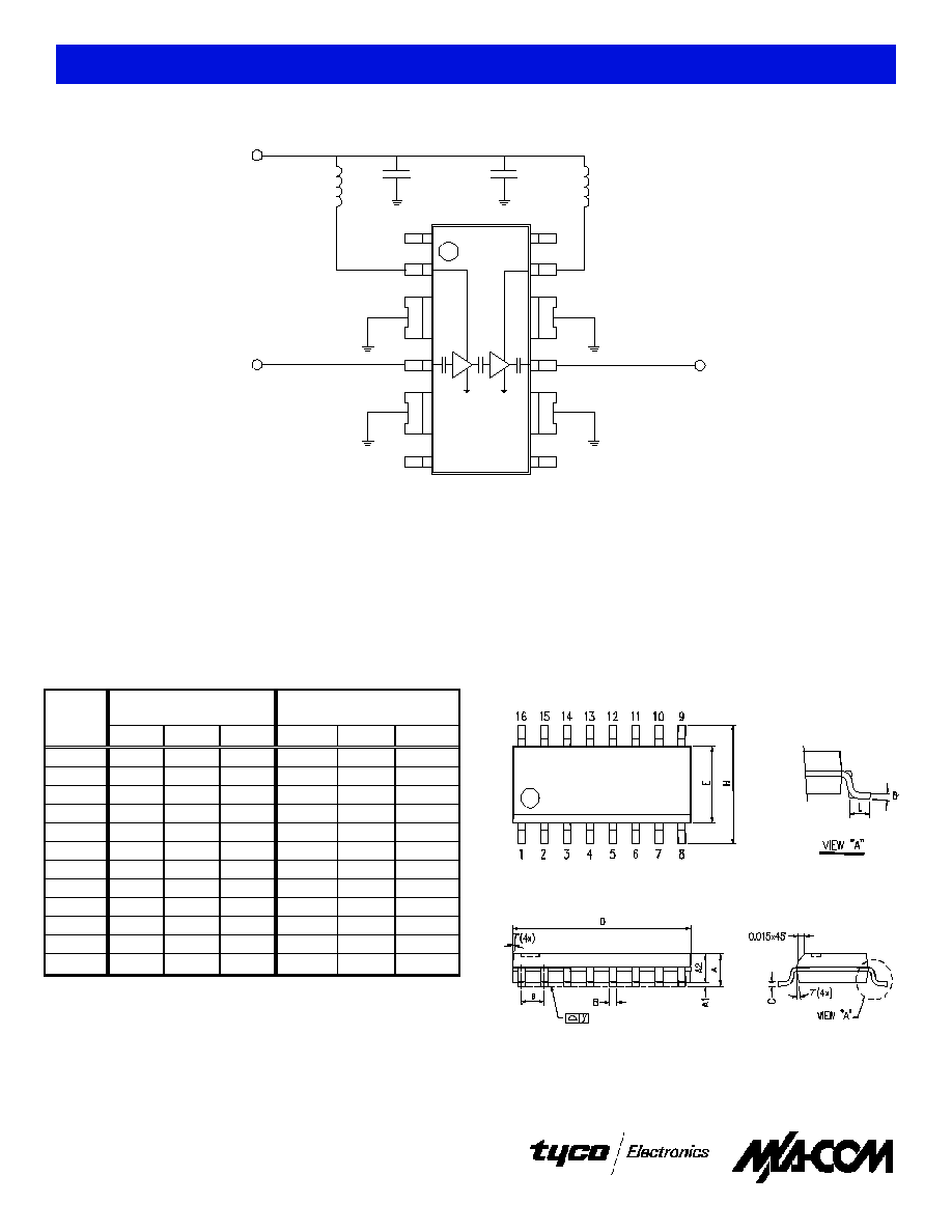
Application Schematic
C2
C1
+V
DD
L2
RF
INPUT
RF
OUTPUT
60mil GETEK Board
L1
N/C
N/C
1
2
3
5
6
8
16
9
11
12
14
15
7
10
4
13
N/C
N/C
List of components:
C1 = C2 = 100 pF DLI multilayer ceramic chip capacitor (C11AH101K5TXL)
L1 = 8.2 nH Coilcraft chip inductor (1008CT.080XKBB)
L2 = 27 nH Coilcraft chip inductor (1008CS.270XKBB)
SOIC-16 Narrow Body Package
Dimensions in
millimeters
Dimensions in inches
Symbol
Min
Nom
Max
Min
Nom
Max
A
1.35
1.60
1.75
0.053
0.063
0.068
A1
0.10
0.25
0.004
0.010
A2
1.45
0.057
B
0.33
0.41
0.51
0.013
0.016
0.020
C
0.19
0.20
0.25
0.0075
0.008
0.0098
D
9.80
9.91
10.01
0.386
0.390
0.394
E
3.80
3.91
4.00
0.150
0.154
0.157
e
1.27
0.050
H
5.79
5.99
6.20
0.228
0.236
0.244
L
0.38
0.71
1.27
0.015
0.028
0.050
y
0.10
0.004
0°
8°
0°
8°
NOTES:
1. Controlling dimension: inch
2. Lead frame material: copper alloy C151
3. Lead thickness after solder plating will be 0.013" maximum
4. Dimension "D" does not include mold flash, protrusions or gate
burrs
5. Dimension "E" does not include interlead flash or protrusions
6. Tolerance: ±0.010" unless otherwise specified