 | ÐлекÑÑоннÑй компоненÑ: MA03501D | СкаÑаÑÑ:  PDF PDF  ZIP ZIP |
/home/web/doc/html/macom/178612
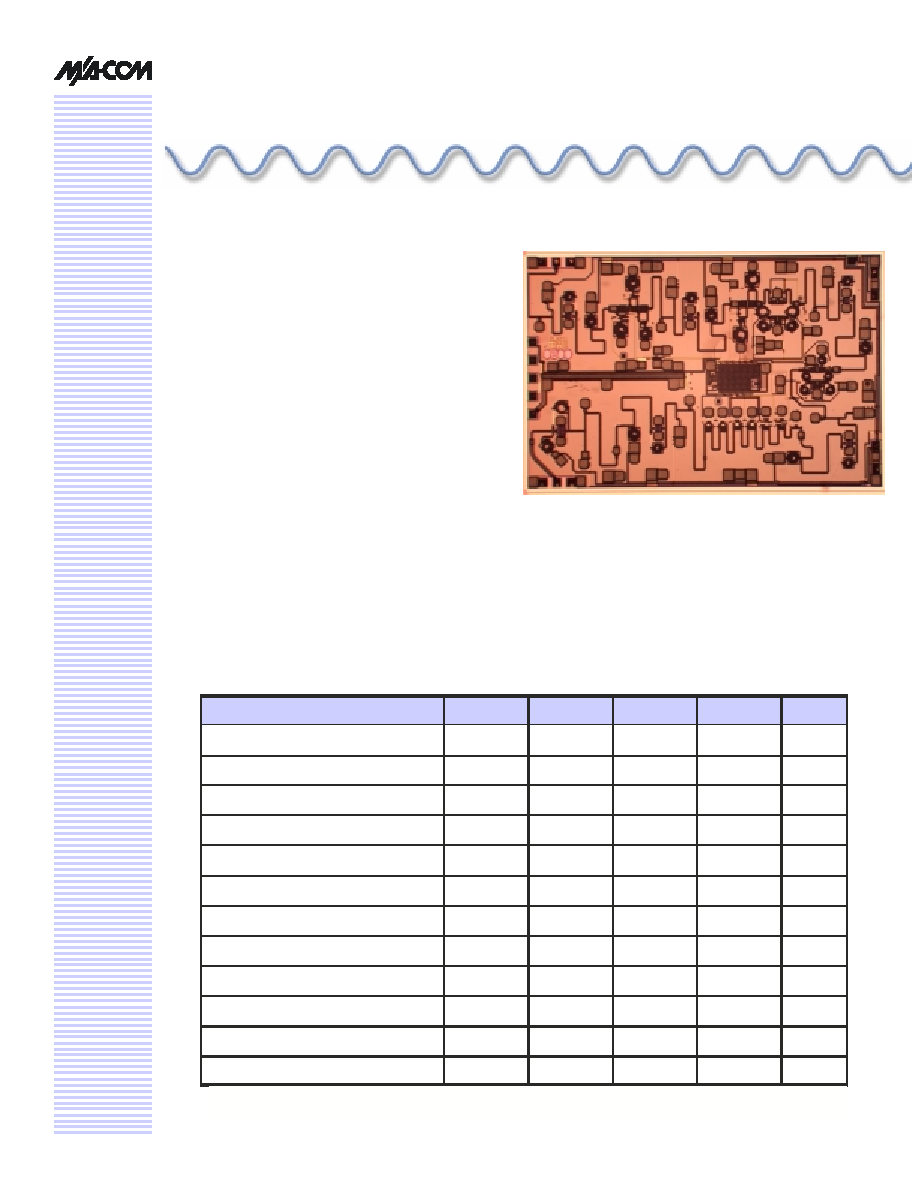
X-Band Gain/Phase Control MMIC
8.0 11.0 GHz
MA03501D
8.0-11.0 GHz Serial Input Control MMIC
V 1.00
Features
E 8.0 to 11.0 GHz Operation
E 6-bit Phase Shifter and 5-bit Attenuator
E Serial Control Input
E 50 Input and Output Impedance
E Self-Aligned MSAG
®
MESFET Process
Primary Applications
E Radar Systems
Electrical Characteristics: T
B
= 25°C
1
, Z
0
= 50
:
:
:
:, V
DD
= 5V, V
GG
= -4V, V
EE
= -4.0
Parameter
Minimum
Typical
Maximum
Units
Bandwidth 8.0
11.0
GHz
Gain 13
18
22.5
dB
1-dB Compression Point
21
dBm
Input Return Loss
10
16
dB
Output Return Loss
10
16
dB
Attenuation Range (5-bits, 0.75dB step)
23
dB
RMS Attenuation Error (Uncorrected)
0.2
dB
0.75
dB
Attenuator
Bit
0.5 0.8 1.0
dB
1.5 dB Attenuator Bit
1.0
1.5
2.0
dB
3 dB Attenuator Bit
2.4
3.0
3.6
dB
6 dB Attenuator Bit
5.0
6.0
7.0
dB
12 dB Attenuator Bit
10.8
12
13.2
dB
Symbol
f
Gn
P1dB
IRL
ORL
Description
The
MA03501D
is a serial control input phase shifter/
attenuator/buffer amplifier MMIC. The on-chip serial to
parallel converter circuitry allows for control of the 6
phase and 5 attenuation bits using a single TTL/CMOS
compatable input. This product is fully matched to 50
ohms on both the input and output.
Each device is 100% RF tested on wafer to ensure
performance compliance. The part is fabricated using
M/A-COM's repeatable, high performance and highly
reliable GaAs Multifunction Self-Aligned Gate (MSAG
®
)
MESFET Process.
1. T
B
= MMIC Base Temperature
V1.00 2/7
X-Band Serial Input Gain/Phase Control MMIC
MA03501D
V 1.00
Specifications subject to change without notice.
Customer Service: Tel. (888)563-3949
Email: macom_adbu_ics@tycoelectronics.com
T
North America:
Tel. (800) 366-2266
T
Asia/Pacific:
Tel.+81-44-844-8296, Fax +81-44-844-8298
T
Europe:
Tel. +44 (1344) 869 595, Fax+44 (1344) 300 020
Visit www.macom.com for additional data sheets and product information.
Absolute Maximum Conditions
1
1. Operation outside of these ranges may reduce product reliability. Operation at other than the typical values may
result in performance outside the guaranteed limits.
Electrical Characteristics: T
B
= 25°C, Z
0
= 50
:
:
:
:, V
DD
= 5V, V
GG
= -4V, V
EE
= -4.0
Parameter
Minimum
Typical
Maximum
Units
Phase Shift Range (6 bits, 5.6 degree step)
354
Deg
RMS Phase Error (Uncorrected)
2
Deg
5.6 Degree Bit
4.0
5.3
7.0
Deg
11.25 Degree Bit
8.0
11.0
13.0
Deg
22.5 Degree Bit
19.0
22.0
24.0
Deg
45 Degree Bit
40.0
44.0
47.0
Deg
90 Degree Bit
85.0
90.0
95.0
Deg
180 Degree Bit
170
180
190
Deg
Gain Variation over all Phase Shifter settings
+/-1.0
dB
Output Third Order Intercept Point
26
dBm
Noise Figure
10
dB
Drain Supply Current
160
275
500
mA
Gate Supply Current
1
10
mA
Digital Power Supply Current
10
20
mA
Input Logic High Current
0.5
mA
Input Logic Low Current
0.1
mA
Timing Delay-Enable Signal to Bit Change
25
nS
Symbol
OTOI
NF
I
DD
I
GG
I
EE
Parameter
Symbol
Absolute Maximum
Units
Input Power
P
IN
12
dBm
Drain Supply Voltage
V
DD
8.0
V
Quiescent DC Power Dissipated (No RF)
P
DISS
2.5
W
Digital Power Supply Voltage
V
EE
-6.0
V
Junction Temperature
T
j
180
°C
Storage Temperature
T
STG
-55 to +150
°C
Gate Supply Voltage
V
GG
-6.0
V
Quiescent Drain Current (No RF)
I
DQ
500
mA
V1.00 3/7
X-Band Serial Input Gain/Phase Control MMIC
MA03501D
V 1.00
Specifications subject to change without notice.
Customer Service: Tel. (888)563-3949
Email: macom_adbu_ics@tycoelectronics.com
T
North America:
Tel. (800) 366-2266
T
Asia/Pacific:
Tel.+81-44-844-8296, Fax +81-44-844-8298
T
Europe:
Tel. +44 (1344) 869 595, Fax+44 (1344) 300 020
Visit www.macom.com for additional data sheets and product information.
Operating Instructions
This device is static sensitive. Please handle
with care. To operate the device, follow these
steps.
1. Apply
V
GG
= -4 V, V
EE
= -4V, V
DD
= 0 V.
2. Ramp
V
DD
to desired voltage, typically 5 V.
3. Adjust
V
GG
to set I
DQ
, (approximately @ 4V).
4. Set
RF
input.
5. Power down in reverse. Turn gate voltage off
last.
Recommended Operating Conditions
2. Maximum MMIC Base Temperature = 150°C-- 31.8°C/W * V
DD
* I
DQ
Characteristic
Symbol
Min
Typ
Max
Unit
Drain Voltage
V
DD
4.0
5.0 6.0 V
Gate Voltage
V
GG
-4.5
-4.0 -3.5 V
Digital Power Supply Voltage
V
EE
-4.2
-4.0 -3.8 V
Input Logic High Voltage
V
IH
3.0
3.5 5.0 V
Input Logic Low Voltage
V
IL
0.0
0.0 0.4 V
Clock Frequency
F
CLK
20 MHz
Junction Temperature
T
J
150
ºC
MMIC Base Temperature
T
B
Note
2
ºC
V1.00 4/7
X-Band Serial Input Gain/Phase Control MMIC
MA03501D
V 1.00
Specifications subject to change without notice.
Customer Service: Tel. (888)563-3949
Email: macom_adbu_ics@tycoelectronics.com
T
North America:
Tel. (800) 366-2266
T
Asia/Pacific:
Tel.+81-44-844-8296, Fax +81-44-844-8298
T
Europe:
Tel. +44 (1344) 869 595, Fax+44 (1344) 300 020
Visit www.macom.com for additional data sheets and product information.
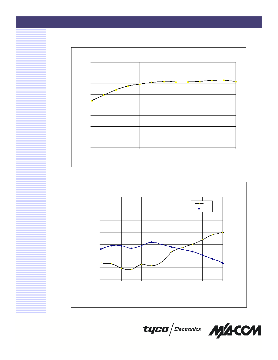
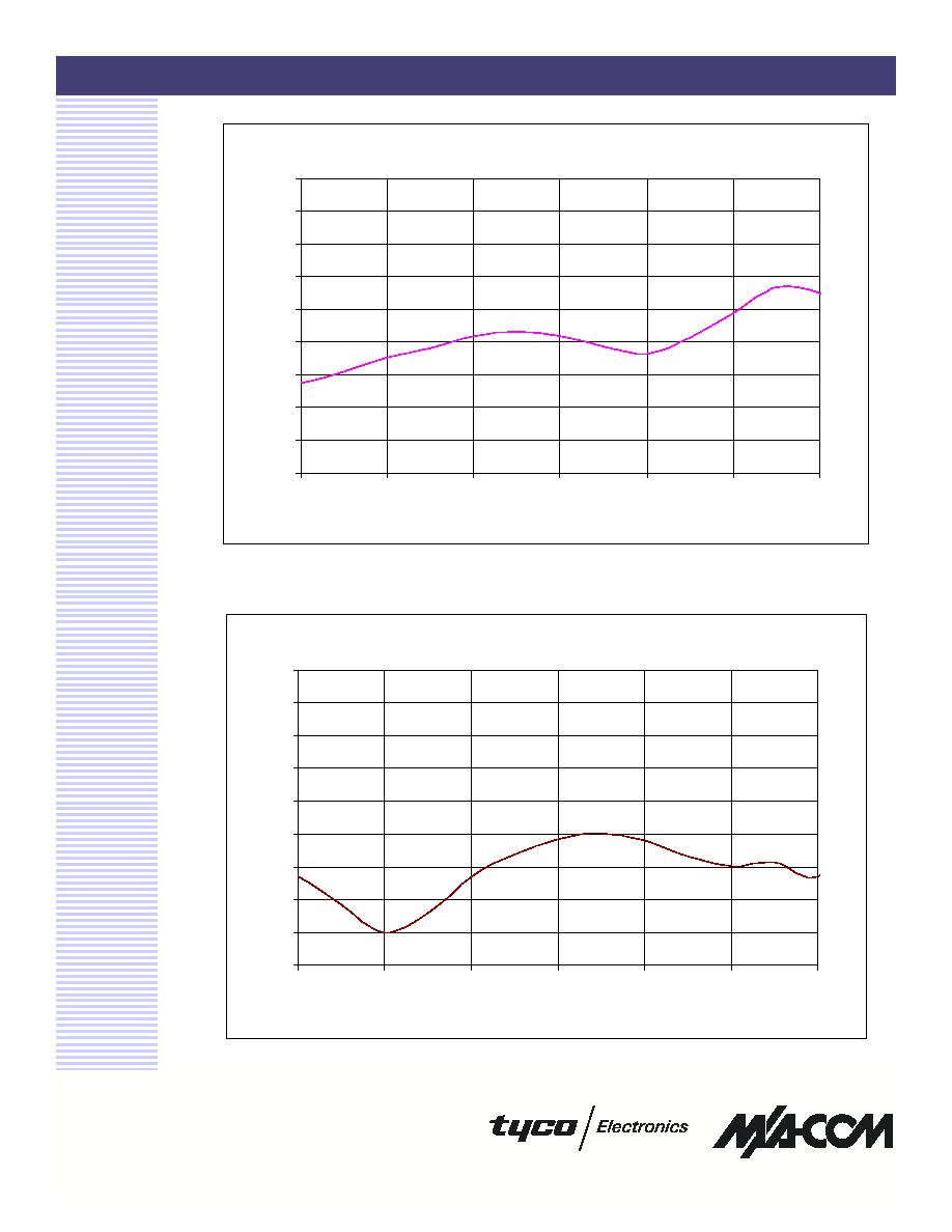
Typical Small Signal Characteristics
(V
DD
=5V, V
GG
=-4V)
Figure 1. Gain
Figure 2. Input and Output Match
14.0
15.0
16.0
17.0
18.0
19.0
20.0
21.0
22.0
8.0
8.5
9.0
9.5
10.0
10.5
11.0
Frequency (GHz)
Ga
i
n
S
2
1
(
d
B
)
-24.0
-22.0
-20.0
-18.0
-16.0
-14.0
-12.0
-10.0
8.0
8.5
9.0
9.5
10.0
10.5
11.0
Frequency (GHz)
I
n
p
u
t
an
d
O
u
t
p
u
t
R
e
t
u
r
n
L
o
s
s S
11
an
d
S
22 (
d
B
)
S22:
S11:
V1.00 5/7
X-Band Serial Input Gain/Phase Control MMIC
MA03501D
V 1.00
Specifications subject to change without notice.
Customer Service: Tel. (888)563-3949
Email: macom_adbu_ics@tycoelectronics.com
T
North America:
Tel. (800) 366-2266
T
Asia/Pacific:
Tel.+81-44-844-8296, Fax +81-44-844-8298
T
Europe:
Tel. +44 (1344) 869 595, Fax+44 (1344) 300 020
Visit www.macom.com for additional data sheets and product information.
0.00
0.05
0.10
0.15
0.20
0.25
0.30
0.35
0.40
0.45
8.0
8.5
9.0
9.5
10.0
10.5
11.0
Frequency (GHz)
R
M
S A
tte
n
u
a
ti
o
n
Er
r
o
r
(d
B
)
Figure 3. RMS Attenuation Error
0.0
0.5
1.0
1.5
2.0
2.5
3.0
3.5
4.0
4.5
8.0
8.5
9.0
9.5
10.0
10.5
11.0
Frequency (GHz)
R
M
S
P
h
a
s
e
E
r
ro
r (
d
e
gre
e
)
Figure 4. RMS Phase Error