Features
n
Specified Performance : 50 MHz to 40 GHz
n
Operational performance: 50 MHz to 50 GHz
n
2.0 dB Typical Insertion Loss at 40 GHz
n
30 dB Typical Isolation at 40 GHz thru 3 Diodes
n
22 dB Typical Isolation at 40 GHz thru 2 Diodes
n
Low Current comsumption :
10 mA for low loss state
0 Volts for Isolation state
n
M/A-COM's unique patent pending AlGaAs
hetero-junction anode technology
n
Silicon Nitride Passivation
n
BCB Impact Protection
Description
M/A-COM's MA4AGSW8-1 is an Aluminum-Gallium- Arsenide
(AlGaAs) anode enhanced, SP8T PIN diode Series Switch.
Operation is accomplished with 10 mA applied to the low loss port
and 0 V for the isolated ports.
M/A-COM's AlGaAs process utilizes a patent pending
hetero-junction technology which produces lower insertion loss
than conventional GaAs devices. These devices are fabricated on
an OMCVD epitaxial wafer using a process designed for high
device uniformity and extremely low parasitics. The diodes exhibit
low series resistance, ( 3
) , low capacitance ( 20 fF ) , and fast
switching speed ( 20 nS ).
The MA4AGSW8-1 device is fully passivated with silicon nitride,
and has an additional layer of a polyamide for impact protection.
This protective coating prevents damage to the junction and the
anode air bridges during assembly and test. RF to DC bias
networks are required. This allows the MA4AGSW8-1 device to
be optimized for a particular operating band.
Applications
The low capacitance of the PIN diodes makes this device ideal for
use in microwave multi-throw switch designs. The low series
resistance of the diodes reduces the insertion loss of the devices at
microwave/millimeter-wave frequencies. These AlGaAs PIN
switches are used as switching arrays on radar systems, optical
switching networks, instrumentation, and other wideband
multi-throw switch assemblies.
AlGaAs SP8T PIN
Diode Series Switch
MA4AGSW8
-
1
V 1.00
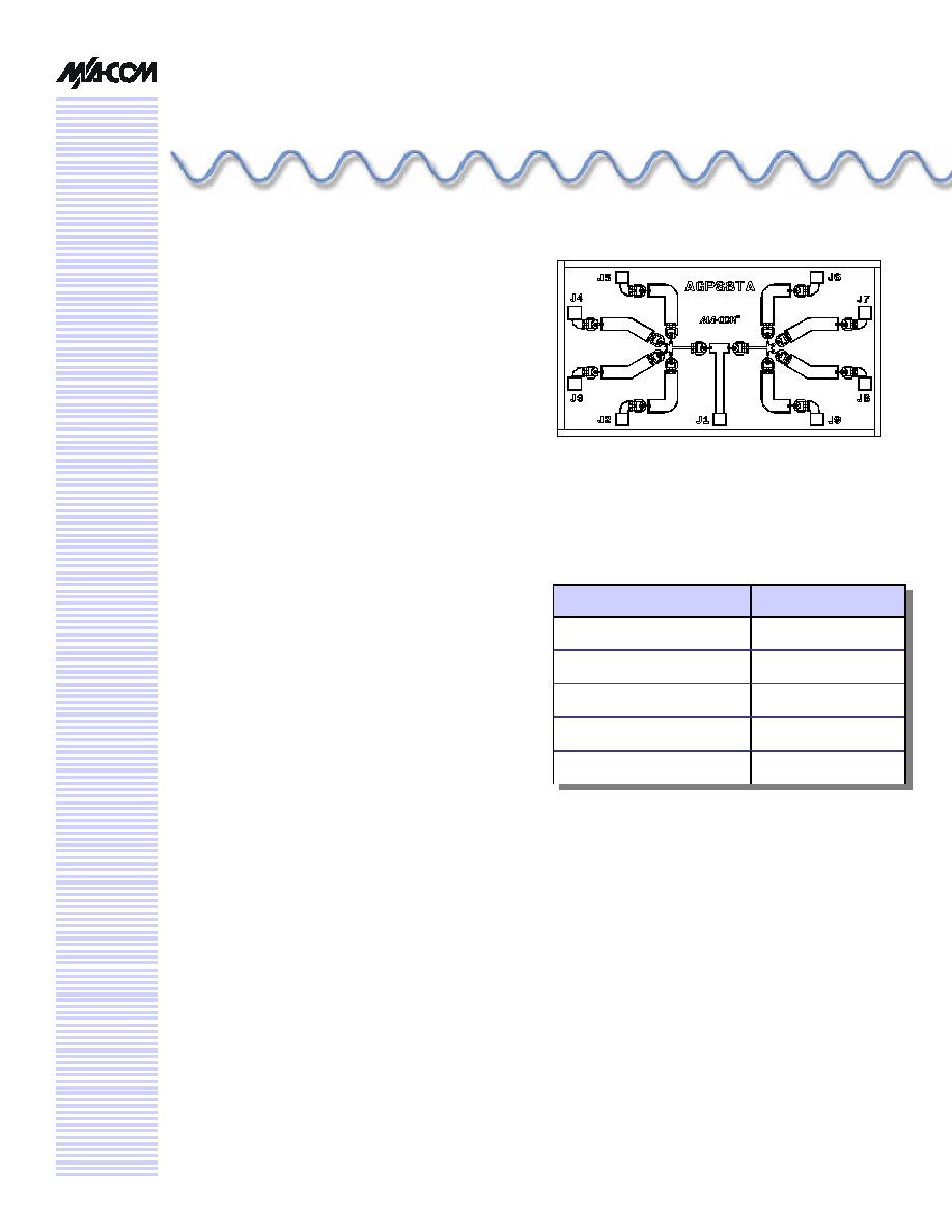
MA4AGSW8-1 Layout
Absolute Maximum Ratings
1
@ TA = +25 ∞C (Unless otherwise
specified)
Parameter
Maximum Rating
Operating Temperature
-55 ∞C to +125 ∞C
Storage Temperature
-65 ∞C to +150 ∞C
Incident C.W. RF Power
+ 23 dBm C. W.
Reverse Voltage
25 V
Bias Current
+/- 30 mA
1. Exceeding any of these values may result in permanent
damage

AlGaAs SP8T PIN Diode Series Switch
MA4AGSW8-1
V 1.00
M/A-COM Inc. and its affiliates reserve the right to make changes to the product(s)
or information contained herein without notice.
Visit www.macom.com for additional data sheets and product information.
n
North America: Tel. (800) 366-2266
n
Asia/Pacific: Tel.+81-44-844-8296, Fax +81-44-844-8298
n
Europe: Tel. +44 (1908) 574 200, Fax+44 (1908) 574 300
2
Typical Driver Connections
Input Port
@J2
@J3
@J4
@J5
@J6
@J7
@J8
@J9
J1
Low Loss
Isolation
Isolation
Isolation
Isolation
Isolation
Isolation
Isolation
J1
Isolation
Low Loss
Isolation
Isolation
Isolation
Isolation
Isolation
Isolation
J1
Isolation
Isolation
Low Loss
Isolation
Isolation
Isolation
Isolation
Isolation
J1
Isolation
Isolation
Isolation
Low Loss
Isolation
Isolation
Isolation
Isolation
Output Ports
J1
Isolation
Isolation
Isolation
Isolation
Low Loss
Isolation
Isolation
Isolation
J1
Isolation
Isolation
Isolation
Isolation
Isolation
Low Loss
Isolation
Isolation
J1
Isolation
Isolation
Isolation
Isolation
Isolation
Isolation
Low Loss
Isolation
J1
Isolation
Isolation
Isolation
Isolation
Isolation
Isolation
Isolation
Low Loss
Electrical Specifications @ T
A
= 25 ∞C, -15 mA Bias Current, and 0 Volts
(On-Wafer Measurements)
RF Specifications
Parameter
Frequency
Minimum
Typical
Maximum
Units
Insertion Loss
0.05 - 18 GHz
18 - 26 GHz
26 - 40 GHz
-
-
-
1.5
1.8
2.0
2.0
2.1
2.3
dB
dB
dB
Isolation
1
0.05 - 18 GHz
18 - 26 GHz
26 - 40 GHz
30
30
30
32
32
32
-
-
-
dB
dB
dB
Input/Output Return Loss
0.05 - 18 GHz
18 - 26 GHz
26 - 40 GHz
10
13
10
15
15
20
-
-
-
dB
dB
dB
Switching Speed
2
10 GHz
-
20
-
ns
1. Low Loss = -15mA applied at the specified Output Port. (A dc ground return at port J1 must be provided)
2. Isolation = 0 Volts applied at the specified Output Ports.
NOTES:
1. Isolation is measured through (3) Diodes from Common Port ( Input ) to Selected Output Port with (1) Opposite Port in Low
Loss. Isolation for (2) Diodes from Common Port ( Input ) to Selected Output with (1) Adjacent Port in Low Loss = 22 dB
Typical.
2. Typical switching speed is measured from 10% to 90% of the detected RF voltage driven by a +/- 5 V TTL compatible driver.
Driver output parallel RC network uses a capacitor between 390 pF - 560 pF and a resistor between 150 - 220 Ohms to
achieve 20 ns rise and fall times.
NOTES:

AlGaAs SP8T PIN Diode Series Switch
MA4AGSW8-1
V 1.00
M/A-COM Inc. and its affiliates reserve the right to make changes to the product(s)
or information contained herein without notice.
Visit www.macom.com for additional data sheets and product information.
n
North America: Tel. (800) 366-2266
n
Asia/Pacific: Tel.+81-44-844-8296, Fax +81-44-844-8298
n
Europe: Tel. +44 (1908) 574 200, Fax+44 (1908) 574 300
3
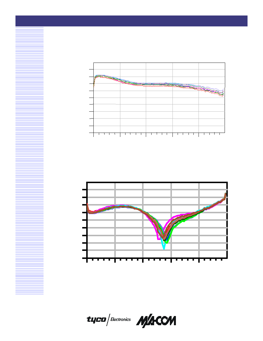
Microwave and Millimeter Wave Performance
10.05
20.05
30.05
40.05
0.05
50.00
-4.5
-4.0
-3.5
-3.0
-2.5
-2.0
-1.5
-1.0
-0.5
-5.0
0.0
freq, GHz
DE
M''.
.S(
2,1
Typical Return Loss
Typical Insertion Loss
10.05
20.05
30.05
40.05
0.05
50.00
-45
-40
-35
-30
-25
-20
-15
-10
-5
-50
0

AlGaAs SP8T PIN Diode Series Switch
MA4AGSW8-1
V 1.00
M/A-COM Inc. and its affiliates reserve the right to make changes to the product(s)
or information contained herein without notice.
Visit www.macom.com for additional data sheets and product information.
n
North America: Tel. (800) 366-2266
n
Asia/Pacific: Tel.+81-44-844-8296, Fax +81-44-844-8298
n
Europe: Tel. +44 (1908) 574 200, Fax+44 (1908) 574 300
4
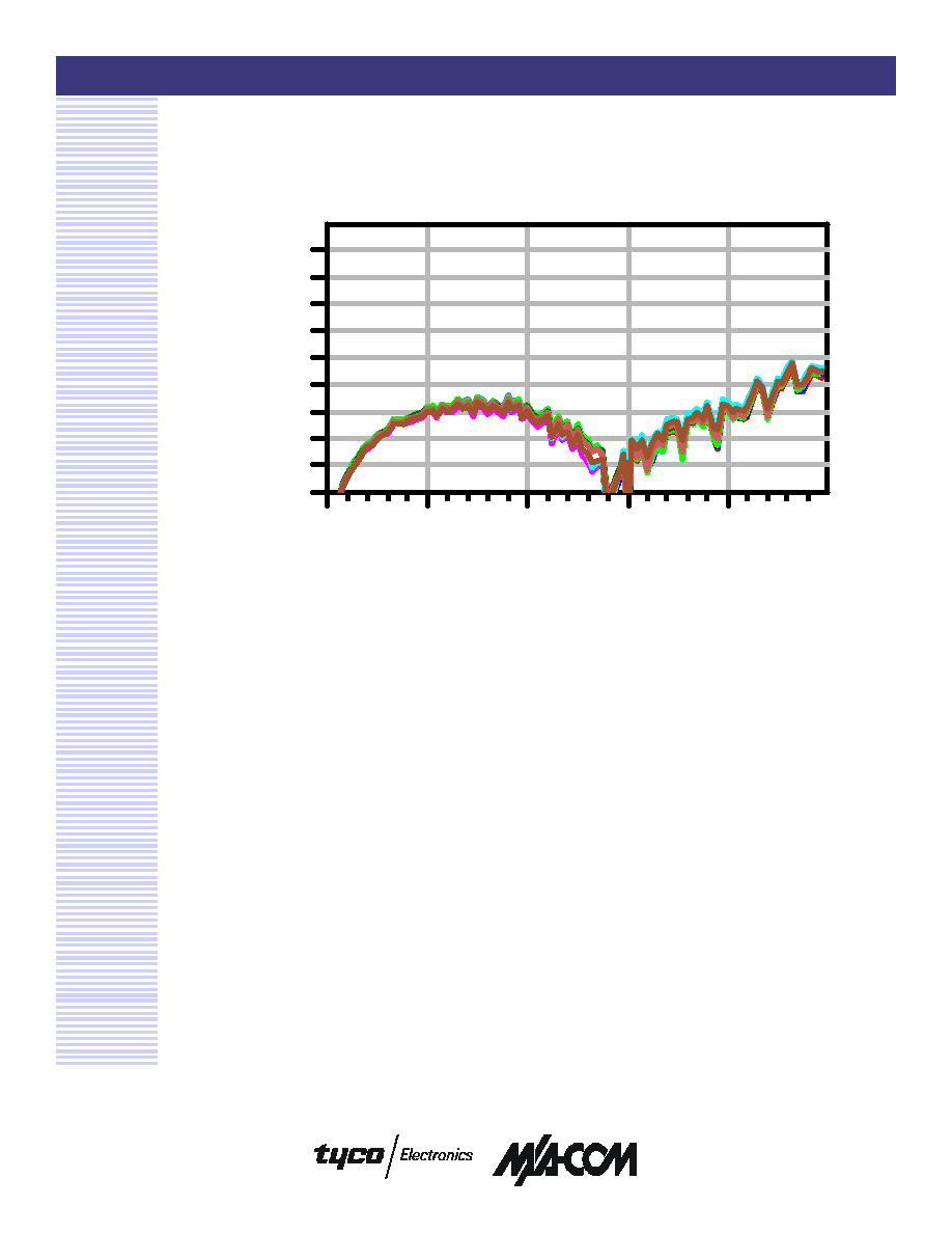
Microwave and Millimeter Wave Performance (cont'd)
Typical Isolation
10.05
20.05
30.05
40.05
0.05
50.00
-45
-40
-35
-30
-25
-20
-15
-10
-5
-50
0

AlGaAs SP8T PIN Diode Series Switch
MA4AGSW8-1
V 1.00
M/A-COM Inc. and its affiliates reserve the right to make changes to the product(s)
or information contained herein without notice.
Visit www.macom.com for additional data sheets and product information.
n
North America: Tel. (800) 366-2266
n
Asia/Pacific: Tel.+81-44-844-8296, Fax +81-44-844-8298
n
Europe: Tel. +44 (1908) 574 200, Fax+44 (1908) 574 300
5
Solder Die Attachment
All die attach and bonding methods should be compatible with
gold metal. Solder which does not scavange gold, such as
80Au/20Sn or Indalloy #2 is recommended. Do not
expose die to a temperature greater than 300 ∞C for more than
10 seconds.
Electrical Conductive Epoxy
Die Attachment
Assembly can be preheated to approximately 125 ∞C. Use a
controlled thickness of approximately 2 mils for best electrical
and thermal conductivity and lower thermal resistance. Cure
epoxy as per manufacturer's schedule. For extended cure
times, temperatures should be kept below 150 ∞C.
Ribbon/Wire Bonding
Wedge thermo compression bonding or ball bonding may be
used to attach ribbons to the bonding pads. Gold ribbons
should be 1/4 x 3 mil sq. for all RF ports for lowest inductance
and best microwave performance.
Assembly Considerations
The following precautions should be observed to avoid
damaging these chips.
Cleanliness
These chips should be handled in a clean environment. Do not
attempt to clean die after installation.
Electro-Static Sensitivity
These Devices are considered ESD Class1. Proper ESD
techniques should be used when handling these devices.
General Handling
The protective polymer coating on the active areas of these die
provides scratch and impact protection, particularly for the
metal airbridge which contacts the diode's anode. Die should
primarily be handled with vacuum pickups, or alternatively
with plastic tweezers.
Mounting Techniques
These AlGaAs devices are designed to be mounted with
electrically conductive silver epoxy or with a lower
temperature solder perform, which is not rich in Sn content.
Operation of the MA4AGSW8-1
The MA4AGSW8-1 switch is designed to operate in systems where lower D.C. current consumption and D.C. operating voltage are
required. The application of either +10 mA or ≠ 10 mA DC bias current to the selected port will provide the low insertion loss state.
Typically this low loss, " ON " bias voltage through (3) series diodes is | 4.5 Volts | maximum. All Isolated Ports can be set to 0 V at
0 mA, or the application of | 5 V | back bias at 0 mA will improve the isolation and switching speed. RF to DC bias networks, (such
as the MA4BN18-40) are required on all RF Ports.
A simple single supply, +5 V, PIN Diode TTL Gate Driver can be used to supply current for loss or 0 V back bias for isolation to
switch the individual RF Ports. In this bias scheme, + 5 V through a current limiting resistor would be applied at the common port and
each RF port would be connected to a TTL Gate. Low loss would occur when the Selected Gate Voltage is 0.5 V @ + 10 mA ,
" TTL 0 " and Isolation would occur when the Selected Gate Voltage is +5V @ 0mA (0 V Back Bias), " TTL 1 ".
For faster switching speeds (< 20 nS) , a +/- 5 V , PIN Diode TTL Driver should be employed to help remove the diode-stored charge
with back bias. In this case, the common port is connected to D.C. Ground. Insertion Loss is achieved with ≠ 10 mA @ ≠ 4.5 V and
Isolation is accomplished by applying + 5 V @ 0mA to the selected RF Ports respectively.
