 | –≠–ª–µ–∫—Ç—Ä–æ–Ω–Ω—ã–π –∫–æ–º–ø–æ–Ω–µ–Ω—Ç: MA4E13171 | –°–∫–∞—á–∞—Ç—å:  PDF PDF  ZIP ZIP |

GaAs Flip Chip
Schottky Barrier Diodes
MA4E1317, MA4E1318
MA4E1319-1, MA4E1319-2
M/A-COM, Inc.
North America:
Tel. (800) 366-2266
s
Asia/Pacific: Tel. +81 (03) 3226-1671
s
Europe: Tel. +44 (1344) 869 595
Fax (800) 618-8883
Fax +81 (03) 3226-1451
Fax +44 (1344) 300 020
1
Specifications Subject to Change Without Notice.
V2.00
Features
Low Series Resistance
Low Capacitance
High Cutoff Frequency
Silicon Nitride Passivation
Polyimide Scratch Protection
Designed for Easy Circuit Insertion
Description
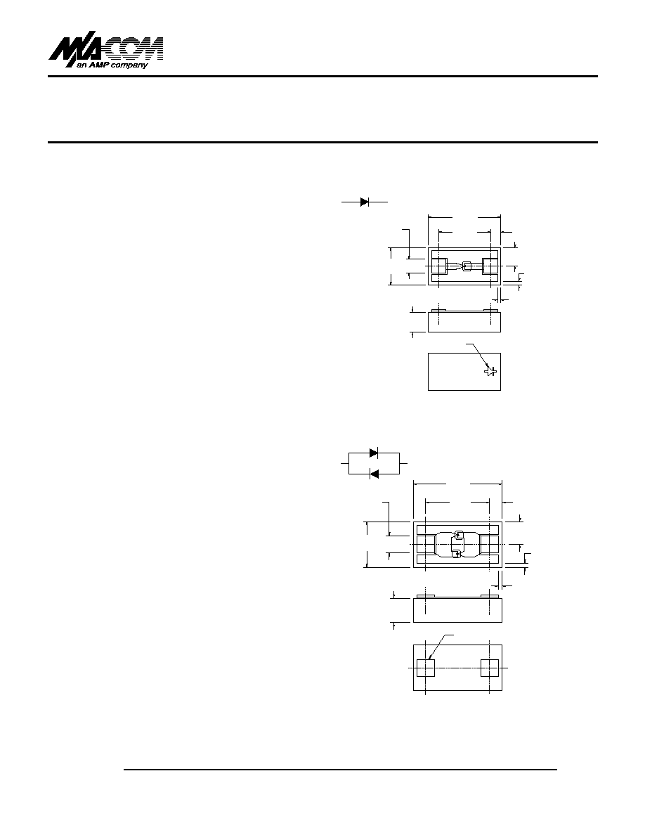
M/A-COM's MA4E1317 single, MA4E1318 anti-parallel
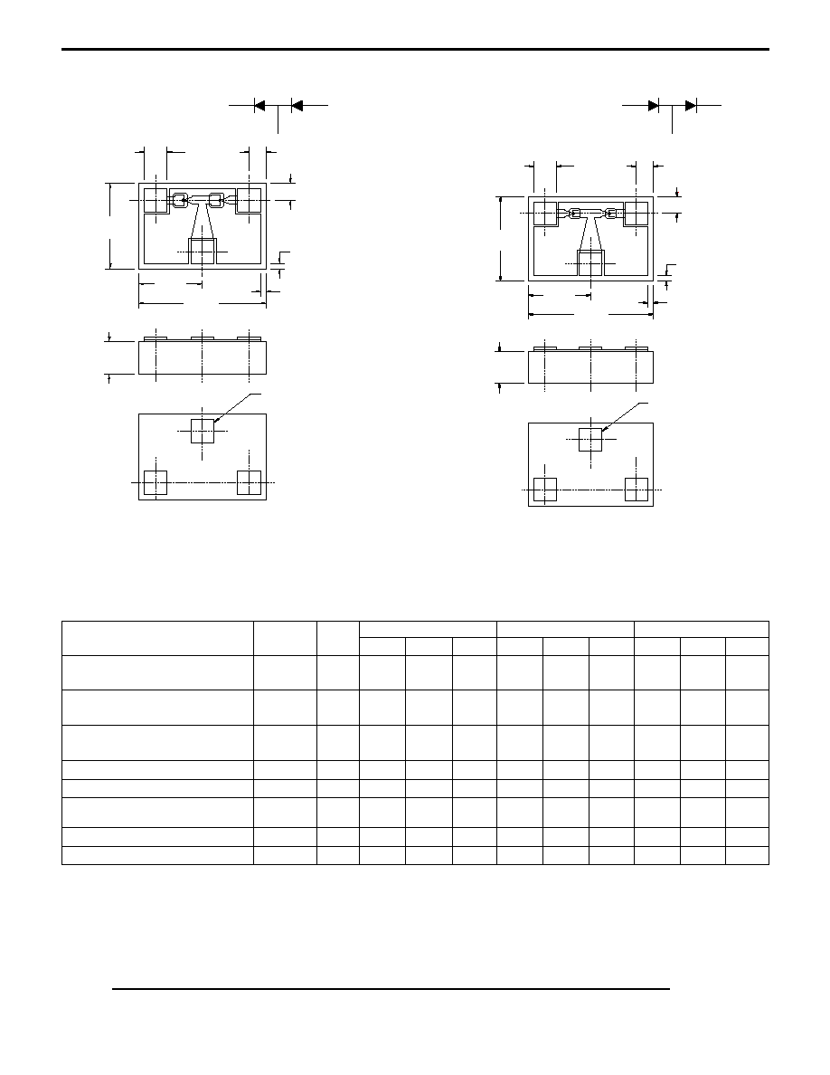
pair, MA4E1319-1 reverse tee and MA4E1319-2 series tee
are gallium arsenide flip chip Schottky barrier diodes.
These diodes are fabricated on OMCVD epitaxial wafers
using a process designed for repeatable electrical
characteristics and extremely low parasitics. The diodes
are fully passivated with silicon nitride and have an
additional layer of polyimide for scratch protection. The
protective coatings prevent damage to the junction
during automated or manual handling. The flip chip
configuration is suitable for pick and place insertion.
Applications
The high cutoff frequency of these diodes allows
use through millimeter wave frequencies. Typical appli-
cations include single and double balanced mixers in
PCN transceivers and radios, police radar detectors, and
automotive radar detectors. The diodes can be used
through 80 GHz.
The MA4E1318 anti-parallel pair is designed for use in
subharmonically pumped mixers. Close matching of the
diode characteristics results in high LO suppression at
the RF input.
MA4E1317
1, 2
Case Style 1198
0.026
(0.65)
0.004 TYP.
(0.10)
0.019
(0.48)
0.007 TYP.
(0.18)
+.001
-.000
0.001
(0.03
TYP.
+.02
-.01
)
POLARITY INDICATOR
0.007
(0.18)
0.013
(0.33)
0.005 SQ.
(0.13) TYP.
+.001
-.000
0.001
(0.03
TYP.
+.02
-.01
)
MA4E1318
1, 2
Case Style 1197
0.026
0.65
0.019
0.48
0.004 TYP.
(0.10)
0.007 TYP.
(0.18)
ALIGNMENT INDICATOR (2 PLCS)
0.013
(0.33)
0.005 SQ.
(0.13) TYP.
0.007
(0.18)
+.001
-.000
0.001
(0.03
TYP.
+.02
-.01
)
+.001
-.000
0.001
(0.03
TYP.
+.02
-.01
)
q
q
q
q
q
q
1. Dimensions in ( ) are in mm.
2. Unless otherwise noted, tolerance are inches ±.001"
(millimeters ±.025 mm)
3. Schematic is for junction side up.

GaAs Flip Chip Schottky Barrier Diodes
MA4E1317, MA4E1318, MA4E1319-1, MA4E1319-2
M/A-COM, Inc.
North America:
Tel. (800) 366-2266
s
Asia/Pacific: Tel. +81 (03) 3226-1671
s
Europe: Tel. +44 (1344) 869 595
Fax (800) 618-8883
Fax +81 (03) 3226-1451
Fax +44 (1344) 300 020
2
Specifications Subject to Change Without Notice.
V2.00
MA4E1319-1
1, 2
Case Style 1199
0.005 SQ.
(0.13) TYP.
+.001
-.000
0.001
(0.03
TYP.
+.02
-.01
)
0.004
(0.10)
TYP.
0.004
(0.10)
TYP.
+.001
-.000
0.001
(0.03
TYP.
+.02
-.01
)
0.014
(0.35)
0.028
(0.70)
0.019
(0.48)
0.007
(0.18)
ALIGNMENT
INDICATOR
(3 PLCS)
0.005 SQ.
(0.13) TYP.
0.004
(0.10) TYP.
0.004
(0.10) TYP.
0.019
(0.48)
0.014
(0.35)
0.028
(0.70)
0.007
(0.18)
+.001
-.000
0.001
(0.03
TYP.
+.02
-.01
)
+.001
-.000
0.001
(0.03
TYP.
+.02
-.01
)
ALIGNMENT
INDICATOR
(3 PLCS)
MA4E1319-2
1, 2
Case Style 1200
MA4E1317
MA4E1318
MA4E1319-1 or -2
Parameters @ Conditions
Symbol
Units
Min.
Typ.
Max.
Min.
Typ.
Max.
Min.
Typ.
Max.
Junction Capacitance
C
j
pF
-
0.020
-
-
0.020
6
-
-
0.020
6
-
0 V @ 1 MHz
Total Capacitance
C
T
pF
0.030
0.045
0.060
0.030
6
0.045
6
0.060
6
0.030
6
0.045
6
0.060
6
0 V @ 1 MHz
4
Junction Capacitance
C
j
pF
-
-
-
-
0.005
0.010
-
0.005
0.010
Difference
Series Resistance @ +10 mA
5
R
S
Ohms
-
4
7
-
4
7
-
4
7
Forward Voltage @ +1 mA
V
F1
Volts
0.60
0.70
0.80
0.60
0.70
0.80
0.60
0.70
0.80
Forward Voltage Difference
V
F
Volts
-
-
-
-
0.005
0.010
-
0.005
0.010
@ 1 mA
Reverse Voltage @ -10 uA
V
R
Volts
4.5
7
-
-
-
-
4.5
7
-
SSB Noise Figure
NF
dB
-
6.5
7
-
-
6.5
7
-
-
6.5
7
-
Electrical Specifications @
T
A
= +25∞C
4. Total capacitance is equivalent to the sum of junction capacitance Cj and parasitic capacitance Cp.
5. Series resistance is determined by measuring the dynamic resistance and subtracting the junction resistance of 2.6 Ohms.
6. Capacitance for the MA4E1318 and MA4E1319-1 or -2 is per Schottky diode.
7. Measured at an LO frequency of 9.375 GHz, with an IF frequency of 300 MHz. LO drive level is +6 dBm for a single Schottky junction.
The IF noise figure contribution (1.5 dB) is included.
1. Dimensions in ( ) are in mm.
2. Unless otherwise noted, tolerance are inches ±.001" (millimeters ±.025 mm)
3. Schematic is for junction side up.

GaAs Flip Chip Schottky Barrier Diodes
MA4E1317, MA4E1318, MA4E1319-1, MA4E1319-2
M/A-COM, Inc.
North America:
Tel. (800) 366-2266
s
Asia/Pacific: Tel. +81 (03) 3226-1671
s
Europe: Tel. +44 (1344) 869 595
Fax (800) 618-8883
Fax +81 (03) 3226-1451
Fax +44 (1344) 300 020
3
Specifications Subject to Change Without Notice.
V2.00
100.00
10.00
1.00
0.10
0.01
0.00
0.20
0.30
0.40
0.50 0.60
0.70
0.80
0.90
1.00
FORWARD CURRENT (
m
A)
FORWARD VOLTAGE (V)
FORWARD CURRENT
VS
FORWARD
VOLTAGE AND TEMPERATURE
Forward Current (mA)
Handling Procedures
The following precautions should be observed to avoid
damaging these chips:
Cleanliness: These chips should be handled in a clean
environment. Do not attempt to clean die after
installation.
Static Sensitivity:
Schottky barrier diodes are ESD
sensitive and can be damaged by static electricity.
Proper ESD techniques should be used when handling
these devices.
General Handling: The protective polymer coating on
the active areas of these die provides scratch protection,
particularly for the metal airbridge which contacts the
anode. Die can be handled with tweezers or vacuum
pickups and are suitable for use with automatic
pick-and-place equipment.
Mounting Techniques
These chips were designed to be inserted onto hard or
soft substrates with the junction side down. They can be
mounted with conductive epoxy or with a low tempera-
ture solder preform. The die can also be assembled with
the junction side up, and wire or ribbon bonds made to
the pads.
Solder Die Attach: Solder which does not scavange
gold, such as Indalloy # 2, is recommended. Sn-Pb based
solders are not recommended due to solder
embrittlement. Do not expose die to a temperature
greater than 235∞C, or greater than 200∞C for longer than
10 seconds. No more than three seconds of scrubbing
should be required for attachment.
Epoxy Die Attach: Assembly can be preheated to 125
to 150∞C. Use a minimum amount of epoxy. Cure epoxy
as per manufacturer's schedule. For extended cure times,
temperatures should be kept below 200∞C.
Absolute Maximum Ratings
1
Parameter
Absolute Maximum
Operating Temperature
-65∞C to +125∞C
Storage Temperature
-65∞C to +150∞C
Incident LO Power
+20 dBm
Incident RF Power
+20 dBm
Mounting Temperature
+235∞C for 10 seconds
1. Exceeding these limits may cause permanent damage.
125∞C 25∞C -50∞C
