B
C
D
E
D
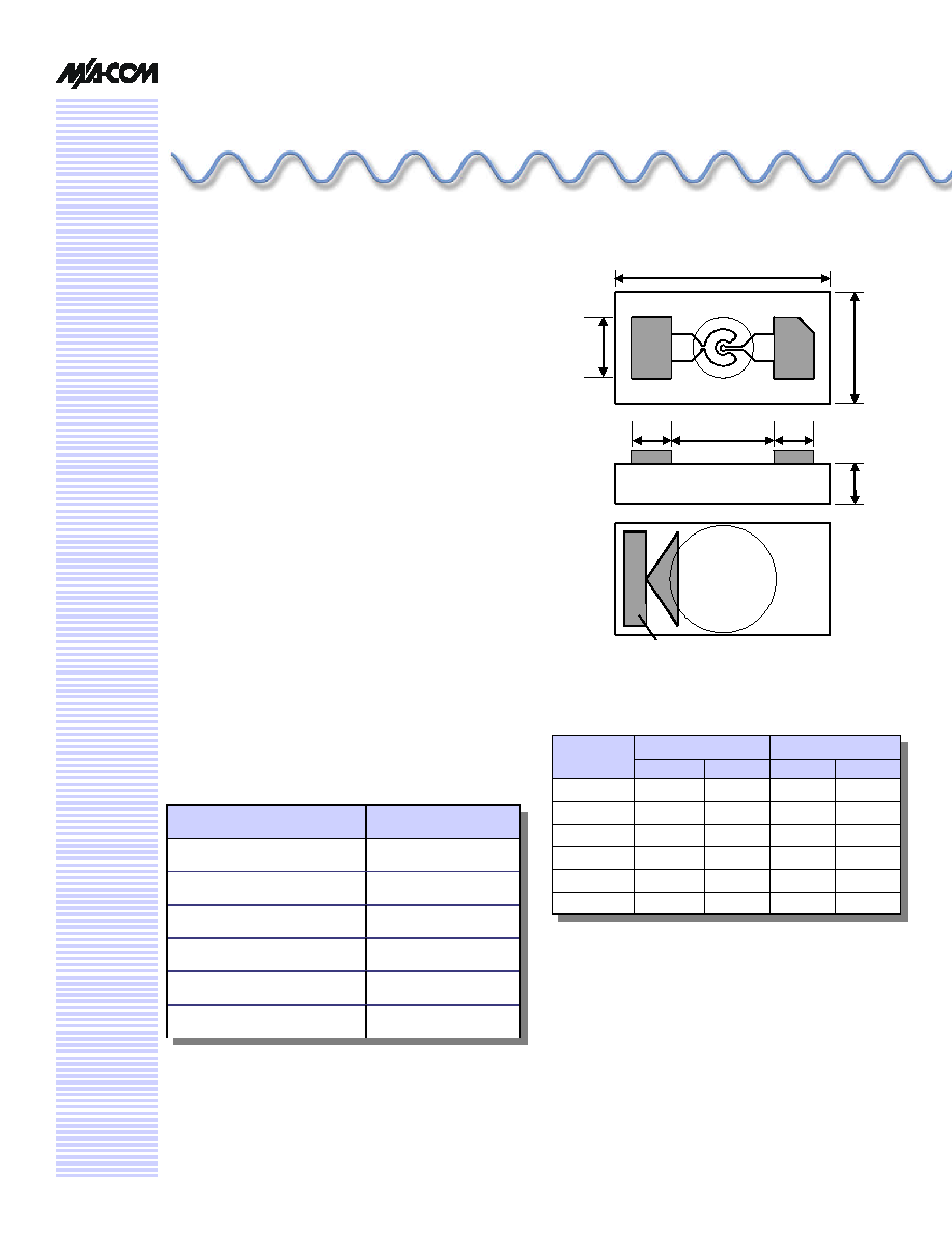
Cathode Mark
Top View
Bottom View
Side View
F
A
Features
n
Low Series Resistance : 1.7
n
Low Capacitance : 50 fF
n
Fast Switching Speed : 20 nS
n
Silicon Nitride Passivation
n
Polyimide Scratch Protection
n
Designed for Automated Pick and Place Insertion
n
Rugged by Design
Description
M/A-COM's MA4FCP Series consists of Silicon Flip Chip PIN
diodes fabricated with M/A-COM's patented HMIC process. This
diode is fabricated on epitaxial wafers using a process designed for
repeatable electrical characteristics and extremely low parasitics.
This diode is fully passivated with Silicon Nitride and has an
additional layer of Polyimide for scratch protection. These
protective coatings prevent damage to the junction during
automated or manual handling. This flip chip configuration is
suitable for pick and place insertion.
Applications
The small 0315 outline and low 0.085 pS RC product, make the
device useful for multi-throw switch and switched phase shifter
circuits requiring < 20 nS switching speeds up to 18 GHz operating
frequency.
Silicon Flip Chip
PIN Diode
MA4FCP305
V 3.00
1269 Outline Drawing
Parameter
Value
Forward Current
100 mA
Reverse Voltage
-40 V
Operating Temperature
-55 �C to +150 �C
Storage Temperature
-55 �C to +150 �C
Dissipated Power
230 mW
Mounting Temperature
+300 �C for 10 seconds
Absolute Maximum Ratings
@ 25 �C
1
1. Exceeding any of these values may result in permanent
damage
Nominal Die Dimensions
Dim
Inches
Millimeters
Min
Max
Min
Max
A
0.0269
0.0289
0.683
0.733
B
0.0135
0.0155
0.343
0.393
C
0.0040
0.0080
0.102
0.203
D
0.0041
0.0061
0.105
0.155
E
0.0124
0.0144
0.315
0.365
F
0.0069
0.0089
0.175
0.225

Silicon Flip Chip PIN Diode
MA4FCP305
V 3.00
M/A-COM Inc. and its affiliates reserve the right to make changes to the product(s)
or information contained herein without notice.
Visit www.macom.com for additional data sheets and product information.
n
North America: Tel. (800) 366-2266
n
Asia/Pacific: Tel.+81-44-844-8296, Fax +81-44-844-8298
n
Europe: Tel. +44 (1344) 869 595, Fax+44 (1344) 300 020
2
1. Total capacitance is equivalent to the sum of junction capacitance Cj and parasitic capacitance, Cp.
2. Series resistance R
S
is equivalent to the total diode series resistance including the junction resistance Rj.
3. Rs and Cp measured on an HP4291A with die mounted in an ODS-186 package.
4. Steady-state thermal resistance measured with die mounted in an ODS-186 package.
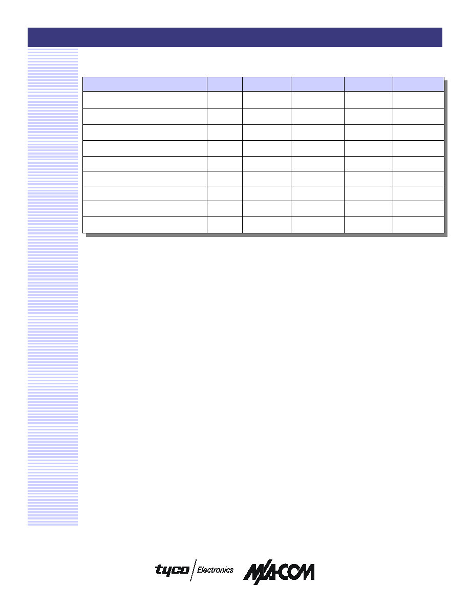
Electrical Specifications @ T
A
= + 25 �C
Parameters @ Conditions
Symbol
Units
Min.
Typ.
Max.
Total Capacitance @ -10 V, 1 MHz
1
C
T
pF
0.060
Total Capacitance @ -10 V, 1 GHz
1,3
C
T
pF
0.050
Series Resistance @ +50 mA
2,3
, 100 MHz
R
S
1.7
Series Resistance @ +50 mA
2,3
, 1 GHz
R
S
2.1
Forward Voltage @ +100 mA
V
F
V
1.05
1.25
Reverse Voltage @ -10
�
A
V
R
V
-40
-50
Reverse Current @ -40 V
I
R
�
A
10
50 - 90% Lifetime @ +10 mA / -6 mA
TL
ns
25
Steady State Thermal Resistance
4
� C/W
640
Mounting Techniques
These devices were designed for insertion onto hard or soft
substrates with the junction side down. They can be mounted
with electrically conductive epoxy or with a low temperature
solder preform. The die can also be assembled with the
junction side up, and wire or ribbon bonds made to the pads.
Solder Die Attach Using
Electrically Conductive Ag Epoxy
and Solder
These chips are designed to be inserted onto hard or soft
substrates with the junction side down. They should be
mounted onto silkscreened circuits using Electrically
Conductive Ag Epoxy, approximately 1-2 mils in thickness
and cured at approximately 90 �C to 150 �C per
manufacturer's schedule . For extended cure times >30
minutes, temperatures must be below 200 �C.
Sn Rich Solders are not recommended due to the Tungsten
Metallization scheme beneath the gold contacts. Indalloy or
80 Au/20 Sn Solders are acceptable. Maximum soldering
temperature must be <300 �C for <10 sec.
Assembly Considerations
The following precautions should be observed for successful
assembly of the die.
Cleanliness
These chips should be handled in a clean environment. Do not
attempt to clean die after installation.
ESD
These devices very susceptible to ESD and are rated Class 0
(0-199 V) per HBM MIL-STD-883, method 3015.7
[C = 100 pF
�
10%, R = 1.5k
�
1%]. Even though tested die
pass 100 V ESD, they must be handled in a static-free
environment
General Handling
The protective polymer coating on the active areas of these
devices provides scratch protection, particularly for the metal
airbridge that contacts the anode. Die can be handled with
tweezers or vacuum pickups and are suitable for use with
automatic pick-and-place equipment.

Silicon Flip Chip PIN Diode
MA4FCP305
V 3.00
M/A-COM Inc. and its affiliates reserve the right to make changes to the product(s)
or information contained herein without notice.
Visit www.macom.com for additional data sheets and product information.
n
North America: Tel. (800) 366-2266
n
Asia/Pacific: Tel.+81-44-844-8296, Fax +81-44-844-8298
n
Europe: Tel. +44 (1344) 869 595, Fax+44 (1344) 300 020
3
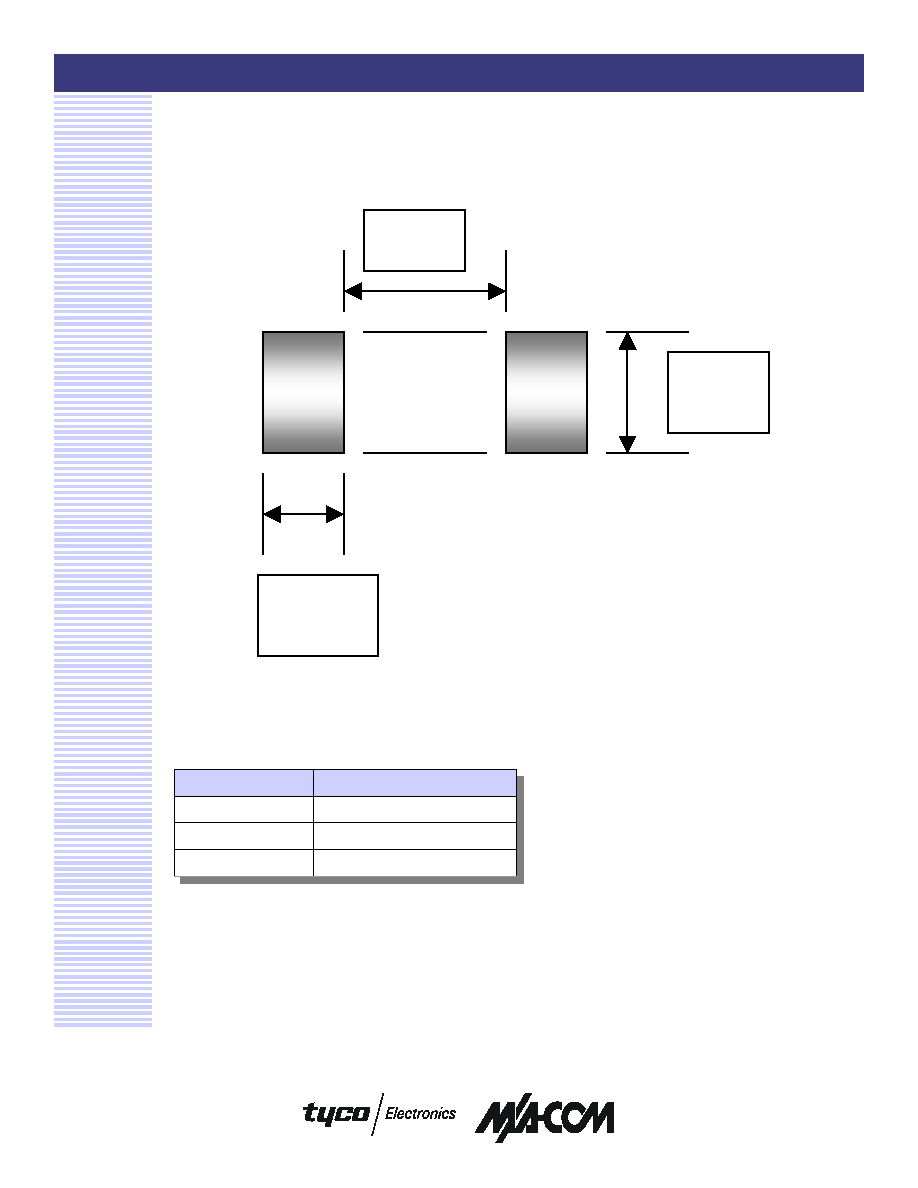
Circuit Mounting Dimensions (Inches)
Ordering Information
Part Number
Package
MA4FCP305
Die in Carrier
MA4FCP305-T
Tape/Reel
MA4FCP305-W
Wafer on Frame
0.012
(2) PL
0.008
(2) PL
0.013

Silicon Flip Chip PIN Diode
MA4FCP305
V 3.00
M/A-COM Inc. and its affiliates reserve the right to make changes to the product(s)
or information contained herein without notice.
Visit www.macom.com for additional data sheets and product information.
n
North America: Tel. (800) 366-2266
n
Asia/Pacific: Tel.+81-44-844-8296, Fax +81-44-844-8298
n
Europe: Tel. +44 (1344) 869 595, Fax+44 (1344) 300 020
4
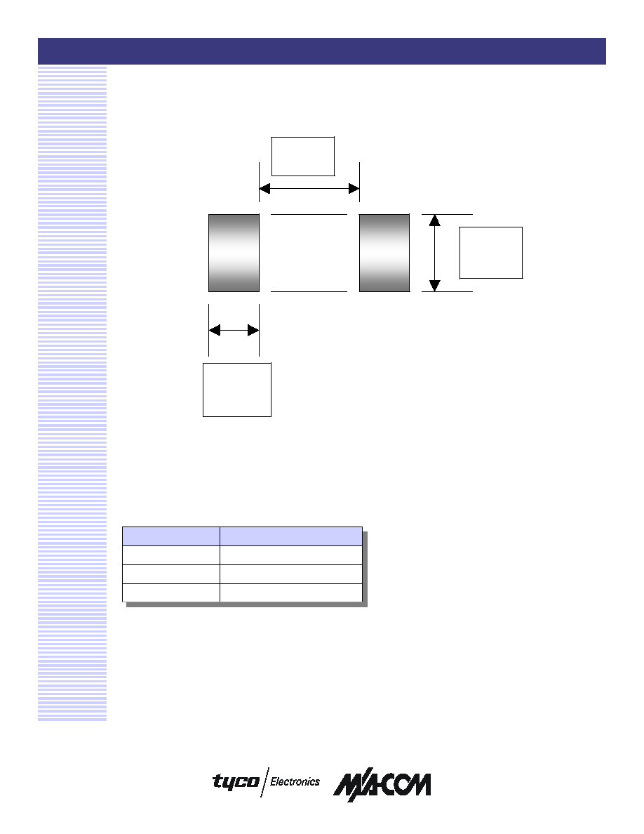
Circuit Mounting Dimensions (Inches)
Ordering Information
Part Number
Package
MA4FCP305
Die in Carrier
MA4FCP305-T
Tape/Reel
MA4FCP305-W
Wafer on Frame
0.012
(2) PL
0.013
0.008
(2) PL
