 | –≠–ª–µ–∫—Ç—Ä–æ–Ω–Ω—ã–π –∫–æ–º–ø–æ–Ω–µ–Ω—Ç: MA4GP907 | –°–∫–∞—á–∞—Ç—å:  PDF PDF  ZIP ZIP |

GaAs Flip-Chip PIN Diodes
V 4.00
Features
n
Low Series Resistance, 4
n
Ultra Low Capacitance, 25 fF
n
High Switching Cutoff Frequency, 40 GHz
n
2 Nanosecond Switching Speed
n
Can be Driven by Buffered TTL
n
Silicon Nitride Passivation
n
Polyimide Scratch Protection
Description
M/A-COM's MA4GP907 is a Gallium Arsenide Flip-Chip PIN
diode.These devices are fabricated on OMCVD epitaxial
wafers using a process designed for high device uniformity and
extremely low parasitics. The diodes exhibit an extremely low
RC Product, ( 0.1 ps ) and 2 nS switching characteristics. They
are fully passivated with silicon nitride and have an additional
layer of a polymer for scratch protection.The protective
coatings prevent damage to the junction and the anode
airbridge during handling.
Applications
The 25 fF capacitance of the MA4GP907 allows use through
mmwave switch and switched phase shifter applications. This
diode is designed for use in pulsed or CW applications, where
single digit nS switching speed is required. For surface mount
assembly, the low capacitance of the MA4GP907 makes it
ideal for use in microwave multithrow switch assemblies,
where the series capacitance of each "off" port adversely loads
the input and affects VSWR.
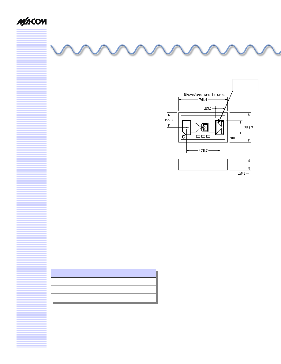
MA4GP907
Package Outline
Top View Is Shown With Diode Junction Up
1
Cathode
Ordering Information
Part Number
Packaging
MA4GP907
Die in Carrier
MA4GP907-T
Tape/Reel
MA4GP907-W
Wafer on Frame

GaAs Flip-Chip PIN Diodes
MA4GP907
V 4.00
M/A-COM Inc. and its affiliates reserve the right to make changes to the product(s)
or information contained herein without notice.
Visit www.macom.com for additional data sheets and product information.
n
North America: Tel. (800) 366-2266
n
Asia/Pacific: Tel.+81-44-844-8296, Fax +81-44-844-8298
n
Europe: Tel. +44 (1344) 869 595, Fax+44 (1344) 300 020
2
Electrical Specifications and RF Data @T
A
= 25 ∞C
Parameters and Test Conditions
Symbol Units
1 MHz & DC
Specifications
Min.
Typ.
Max.
Min.
Typ.
Max.
Total Capacitance at -10 V
Ct
pF
0.025 0.030
0.025
Forward Resistance at +10mA
Rs
Ohms
5.2
7.0
4.2
Forward Voltage at +10mA
Vf
Volts
1.33
1.45
Reverse Breakdown Voltage at -10uA
3
Vb
Volts
-50
-45
Switching Speed (10 to 90% RF Voltage)
4
& (90 to 10% RF Voltage)
4
Trise
Tfall
nS
2
10 GHz Reference
Data
1,2
1. Capacitance is determined by measuring Single Series Diode Isolation in a 50 ohm line at 10 GHz.
2. Forward Series Resistance is determined by measuring Single Series Diode Insertion Loss in a 50 ohm line
at 10 GHz.
3. Reverse current will not exceed 10 microamperes at the Maximum Voltage Rating.
4. Switching speed is measured between 10% and 90% or 90% to 10% RF Voltage for a Single Series Mounted Diode.
Driver delay is Not included.
Notes:
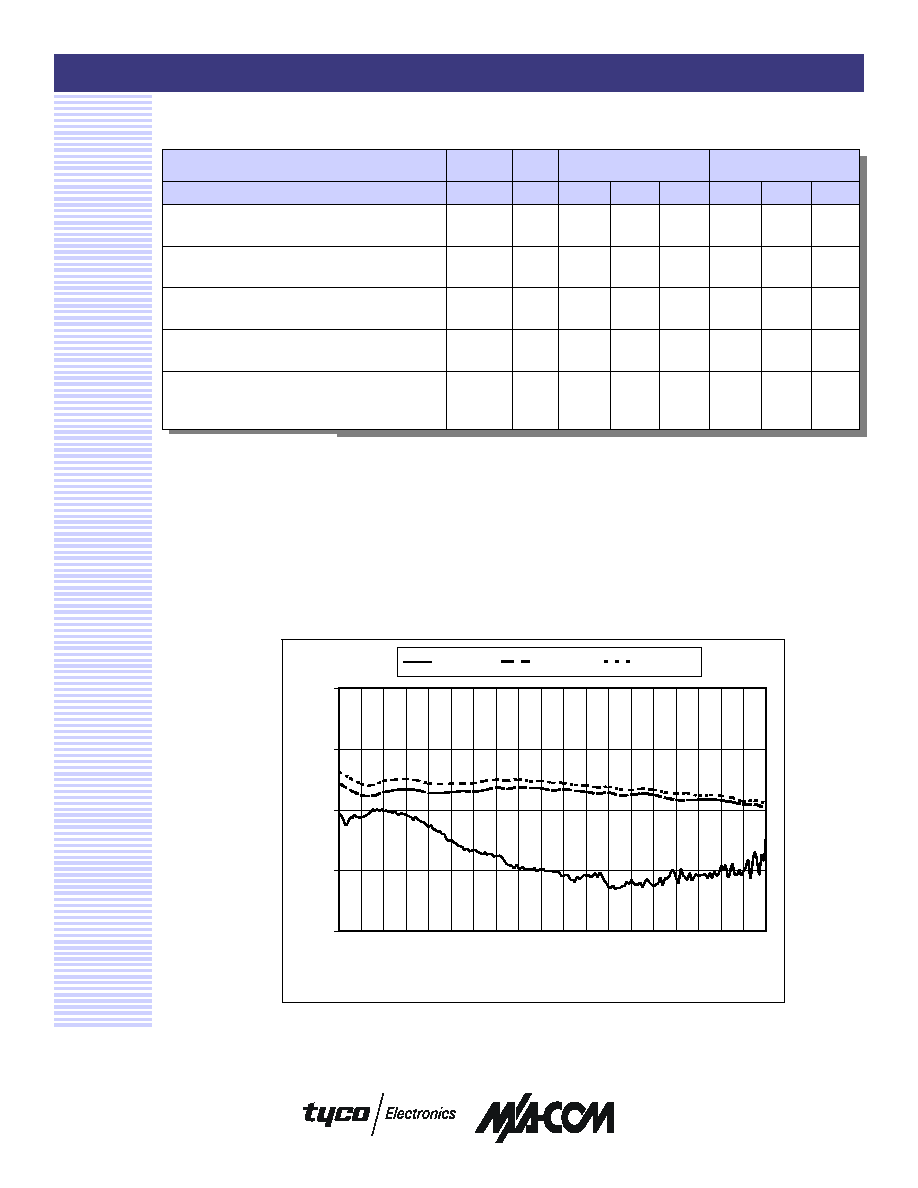
Single Series Diode Insertion Loss vs Frequency
-0.8
-0.6
-0.4
-0.2
0.0
2 4 6 8 10 12 14 16 18 20 22 24 26 28 30 32 34 36 38 40
Frequency (GHz)
Insertion Loss (dB)
I. Loss @5mA
I. Loss @15mA
I. Loss @50mA

GaAs Flip-Chip PIN Diodes
MA4GP907
V 4.00
M/A-COM Inc. and its affiliates reserve the right to make changes to the product(s)
or information contained herein without notice.
Visit www.macom.com for additional data sheets and product information.
n
North America: Tel. (800) 366-2266
n
Asia/Pacific: Tel.+81-44-844-8296, Fax +81-44-844-8298
n
Europe: Tel. +44 (1344) 869 595, Fax+44 (1344) 300 020
3
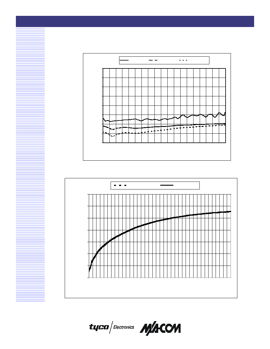
Single Series Diode Return Loss vs Frequency
-40.0
-35.0
-30.0
-25.0
-20.0
-15.0
-10.0
-5.0
0.0
2 4 6 8 10 12 14 16 18 20 22 24 26 28 30 32 34 36 38 40
Frequency (GHz)
Return Loss (dB)
R. Loss @5mA
R. Loss @15mA
R. Loss @50mA
Single Series Diode Isolation vs Frequency
-35.0
-30.0
-25.0
-20.0
-15.0
-10.0
-5.0
0.0
2 4
6 8 10 12 14 16 18 20 22 24 26 28 30 32 34 36 38 40
Frequency ( GHz )
Isolation (dB)
Isolation @ -10V
Isolation @ 0V

GaAs Flip-Chip PIN Diodes
MA4GP907
V 4.00
M/A-COM Inc. and its affiliates reserve the right to make changes to the product(s)
or information contained herein without notice.
Visit www.macom.com for additional data sheets and product information.
n
North America: Tel. (800) 366-2266
n
Asia/Pacific: Tel.+81-44-844-8296, Fax +81-44-844-8298
n
Europe: Tel. +44 (1344) 869 595, Fax+44 (1344) 300 020
4
Parameter
Maximum Ratings
Operating Temperature
-65 ∞C to +125 ∞C
Storage Temperature
-65 ∞C to +150 ∞C
Dissipated RF & DC Power
50 mW
RF C.W. Incident Power
+ 23 dBm C.W.
Mounting Temperature
+300 ∞C for 10 seconds
Absolute Maximum Ratings
5
5. Exceeding any of these values may result in permanent
damage
Device Installation Procedures
The following guidelines should be observed to avoid damag-
ing GaAs Flip-Chips.
Cleanliness
These devices should be handled in a clean environment.
Do Not attempt to clean die After installation.
Static Sensitivity
Gallium arsenide PIN diodes are ESD sensitive and can be
damaged by static electricity. Proper ESD techniques should
be used when handling these devices. These devices are rated
Class 0, (0-199 V) per HBM MIL-STD-883, method 3015.7
[C = 100pF ±10%, R = 1.5kW ±1%]. Even though tested die
pass 50V ESD, they must be handled in a static-free environment.
General Handling
These devices have a polymer layer which provides scratch
protection for the junction area and the anode air bridge. Die
can be handled with plastic tweezers or picked and placed
with a #27 tip vacuum pencil.
Assembly Requirements Using
Electrically Conductive Ag Epoxy
and Solder
These chips are designed to be inserted onto hard or soft sub-
strates with the junction side down. They should be mounted
onto silkscreened circuits using Electrically Conductive Ag
Epoxy, approximately 1-2 mils in thickness and cured at ap-
proximately 90
∞
C to 150
∞
C per manufacturer's schedule.
For extended cure times > 30 minutes, temperatures must be
below 200
∞
C.
Sn Rich Solders are not recommended due to the Tungsten
Metallization scheme beneath the gold contacts. Indalloy or
80 Au/20 Sn Solders are acceptable. Maximum soldering
temperature must be < 300
∞
C for < 10 sec.
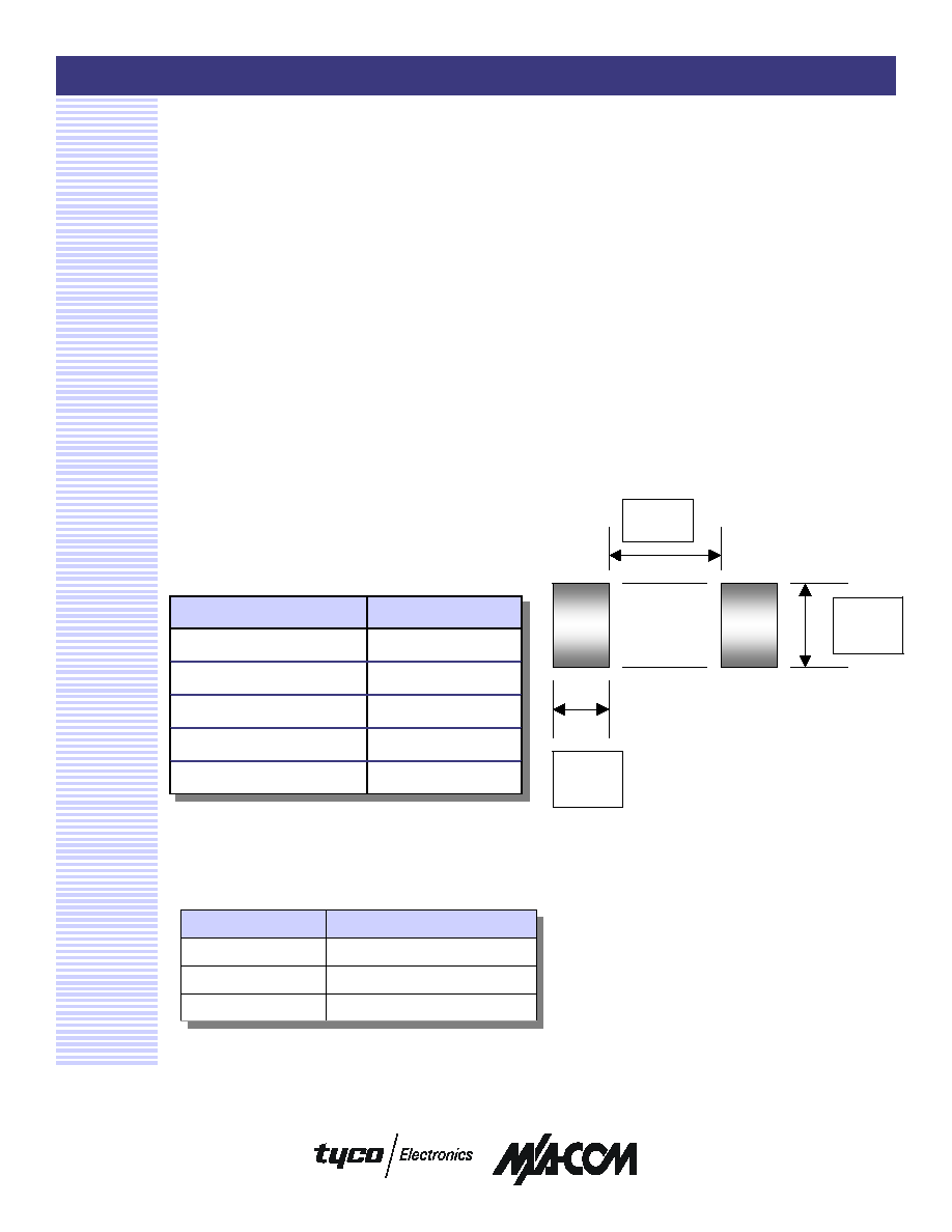
Circuit Mounting Dimensions
(Inches)
0.012
(2) PL
0.008
(2) PL
0.013
Ordering Information
Part Number
Package
MA4GP907
Die in Carrier
MA4GP907-T
Tape and Reel
MA4GP907-W
Wafer on Frame
