/home/web/doc/html/macom/178736

Features
· Low Noise Figure
· High IP
3
· Single +3 V or +5 V Supply Voltage
· Little performance change over Temperature
Description
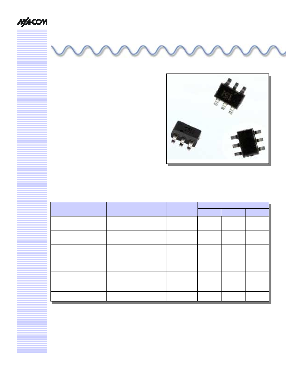
M/A-COM's MAALSS0012 broadband gain stage is a
GaAs MMIC amplifier in a low-cost miniature SOT-363
surface mount plastic package. The MAALSS0012
employs a monolithic 1-stage self-biased design featuring a
convenient 50 ohm input/output impedance that minimizes
the number of external components required. The device
typically runs from a single 3.0 volt supply and may also
operate at any voltage up to 5.0 volts for improved power
performance. Its broadband design provides usable
performance from 200 to 3000 MHz.
M/A-COM fabricates the MAALSS0012 using an E/D
MESFET process to realize low noise and high dynamic
range. The process features full passivation for
performance and reliability.
Miniature Broadband Gain Stage
200 - 3000 MHz
MAALSS0012
V 9.00
Electrical Specifications:
Z
0
= 50 , T
A
= 25 °C
Parameter
Test Conditions
Units
+5 V
Min.
Typ.
Max.
Gain
1
F = 0.9 GHz
F = 1.9 GHz
F = 3.0 GHz
dB
dB
dB
--
11.0
--
14.2
12.0
9.6
--
13.0
--
Noise Figure
2
F = 0.9 GHz
F = 1.9 GHz
F = 3.0 GHz
dB
dB
dB
--
--
--
1.5
1.5
1.6
--
2.0
--
Input Return Loss
F = 0.9 GHz
F = 1.9 GHz
F = 3.0 GHz
dB
dB
dB
--
--
--
9.4
13.2
14.7
--
--
--
Output Return Loss
F = 0.9 GHz
F = 1.9 GHz
F = 3.0 GHz
dB
dB
dB
--
--
--
9.7
15.5
33.0
--
--
--
1dB Compression
200 3000 MHz
dBm
--
21
--
Output IP
3
200 3000 MHz
dBm
--
36
--
Current
--
mA
50
87
100
1. Gain varies at -0.0025 dB/°C typical.
2. Noise figure varies at 0.007 dB/°C typical.
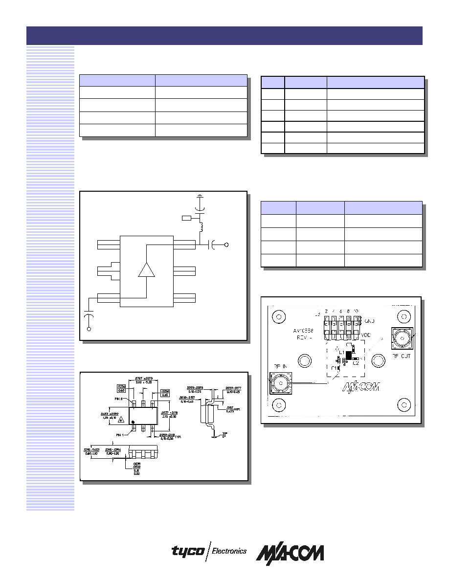
SC-70 6-Lead (SOT-363) Package

Miniature Broadband Gain Stage, 200 - 3000 MHz
MAALSS0012
V 9.00
M/A-COM Inc. and its affiliates reserve the right to make changes to the product(s)
or information contained herein without notice.
Visit www.macom.com for additional data sheets and product information.
!
North America:
Tel. (800) 366-2266
!
Asia/Pacific:
Tel.+81-44-844-8296, Fax +81-44-844-8298
!
Europe:
Tel. +44 (1908) 574200, Fax+44 (1908) 574300
2
External Circuitry
Part
Value
Purpose
C1
39 pF
Input DC Block
C2
39 pF
Output DC Block
C3
470 pF
RF Bypass
L1
12 nH
RF Choke/Tuning
Absolute Maximum Ratings
3
Parameter
Absolute Maximum
RF Input Power
15 dBm
Voltage 6.0
volts
Operating Temperature
-40 °C to +85 °C
Storage Temperature
-65 °C to +150 °C
3. Exceeding any one or combination of these limits may cause
permanent damage to this device.
5. Series inductor and decoupling capacitor recommended
on pin 6.
PIN Configuration
PIN
Function
Description
1
GND
Ground
2
GND
Ground
3
RF In
RF input
4
GND
Ground
5
GND
Ground
6
5
RF Out/V
DD
RF output & drain voltage input
Recommended PCB Configuration
SC-70 6-Lead (SOT-363) Package
4
4. See JEDEC MO-203 VAR AB for additional dimensions and
tolerances.
Functional Block Diagram
Pin 1
GND
GND
GND
GND
Paddle
Input
C1
Output
L1
Vdd
C3
C2

Miniature Broadband Gain Stage, 200 - 3000 MHz
MAALSS0012
V 9.00
M/A-COM Inc. and its affiliates reserve the right to make changes to the product(s)
or information contained herein without notice.
Visit www.macom.com for additional data sheets and product information.
!
North America:
Tel. (800) 366-2266
!
Asia/Pacific:
Tel.+81-44-844-8296, Fax +81-44-844-8298
!
Europe:
Tel. +44 (1908) 574200, Fax+44 (1908) 574300
3
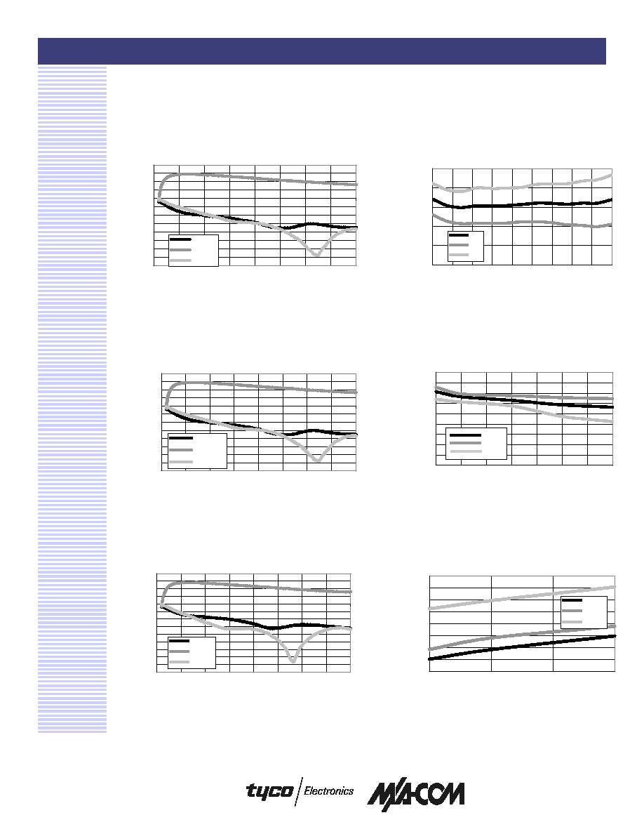
Typical Performance Curves
S-Parameters V
DD
@ 5.0 V, T = 25 °C
-40
-35
-30
-25
-20
-15
-10
-5
0
5
10
15
20
0.0
0.5
1.0
1.5
2.0
2.5
3.0
3.5
4.0
FREQUENCY (GHz)
(d
B)
S11 5.0V
S21 5.0V
S22 5.0V
S-Parameters V
DD
@ 5.0 V, T = - 40 °C
-40
-35
-30
-25
-20
-15
-10
-5
0
5
10
15
20
0.0
0.5
1.0
1.5
2.0
2.5
3.0
3.5
4.0
FREQUENCY (GHz)
(d
B
)
S11 5.0V
S21 5.0V
S22 5.0V
S-Parameters V
DD
@ 5.0 V, T = 70 °C
-45
-40
-35
-30
-25
-20
-15
-10
-5
0
5
10
15
20
0.0
0.5
1.0
1.5
2.0
2.5
3.0
3.5
4.0
FREQUENCY (GHz)
(d
B
)
S11 5.0V
S21 5.0V
S22 5.0V
Noise Figure @ 5.0 Volts
0.0
0.5
1.0
1.5
2.0
2.5
0.4
0.8
1.2
1.6
2.0
2.4
2.8
3.2
3.6
4.0
FREQUENCY (GHz)
NF
(
d
B)
25C
-40C
85C
P
1dB
V
DD
= 5.0 Volts
15
16
17
18
19
20
21
22
23
24
0.5
1.0
1.5
2.0
2.5
3.0
3.5
4.0
FREQUENCY (GHz)
P
1
dB
(dBm)
25C
-40C
85C
Output IP
3
at 25 °C
30
31
32
33
34
35
36
37
38
0.5
1.0
1.5
2.0
FREQUENCY (GHz)
IP
3
(d
Bm)
IP3 2.7V
IP3 3.0V
IP3 5.0V

Miniature Broadband Gain Stage, 200 - 3000 MHz
MAALSS0012
V 9.00
M/A-COM Inc. and its affiliates reserve the right to make changes to the product(s)
or information contained herein without notice.
Visit www.macom.com for additional data sheets and product information.
!
North America:
Tel. (800) 366-2266
!
Asia/Pacific:
Tel.+81-44-844-8296, Fax +81-44-844-8298
!
Europe:
Tel. +44 (1908) 574200, Fax+44 (1908) 574300
4
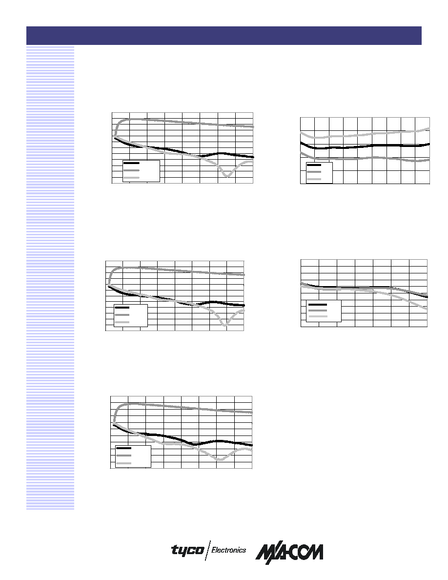
Typical Performance Curves (Cont'd)
S-Parameters V
DD
@ 3.0 V, T = 70 °C
-35
-30
-25
-20
-15
-10
-5
0
5
10
15
20
0.0
0.5
1.0
1.5
2.0
2.5
3.0
3.5
4.0
FREQUENCY (GHz)
(dB
)
S11 3.0V
S21 3.0V
S22 3.0V
Noise Figure @ 3.0 Volts
0.0
0.5
1.0
1.5
2.0
2.5
0.4
0.8
1.2
1.6
2.0
2.4
2.8
3.2
3.6
4.0
FREQUENCY (GHz)
NF
(d
B)
25C
-40C
85C
P
1dB
V
DD
= 3.0 Volts
15.0
15.5
16.0
16.5
17.0
17.5
18.0
18.5
19.0
19.5
20.0
0.5
1.0
1.5
2.0
2.5
3.0
3.5
4.0
FREQUENCY (GHz)
P
1
dB
(d
Bm)
25C
-40C
85C
S-Parameters V
DD
@ 3.0 V, T = 25 °C
-40
-35
-30
-25
-20
-15
-10
-5
0
5
10
15
20
0.0
0.5
1.0
1.5
2.0
2.5
3.0
3.5
4.0
FREQUENCY (GHz)
(d
B
)
S11 3.0V
S21 3.0V
S22 3.0V
S-Parameters V
DD
@ 3.0 V, T = - 40° C
-40
-35
-30
-25
-20
-15
-10
-5
0
5
10
15
20
0.0
0.5
1.0
1.5
2.0
2.5
3.0
3.5
4.0
FREQUENCY (GHz)
(d
B
)
S11 3.0V
S21 3.0V
S22 3.0V

Miniature Broadband Gain Stage, 200 - 3000 MHz
MAALSS0012
V 9.00
M/A-COM Inc. and its affiliates reserve the right to make changes to the product(s)
or information contained herein without notice.
Visit www.macom.com for additional data sheets and product information.
!
North America:
Tel. (800) 366-2266
!
Asia/Pacific:
Tel.+81-44-844-8296, Fax +81-44-844-8298
!
Europe:
Tel. +44 (1908) 574200, Fax+44 (1908) 574300
5
Typical Performance Curves (Cont'd)
P
1dB
V
DD
= 2.7 Volts
12
13
14
15
16
17
18
19
20
0.5
1.0
1.5
2.0
2.5
3.0
3.5
4.0
FREQUENCY (GHz)
P
1
dB
(d
Bm
)
25C
-40C
85C
S-Parameters V
DD
@ 2.7 V, T = 70 °C
-30
-25
-20
-15
-10
-5
0
5
10
15
20
0.0
0.5
1.0
1.5
2.0
2.5
3.0
3.5
4.0
FREQUENCY (GHz)
(d
B
)
S11 2.7V
S21 2.7V
S22 2.7V
Noise Figure @ 2.7 Volts
0.0
0.5
1.0
1.5
2.0
2.5
0.4
0.8
1.2
1.6
2
2.4
2.8
3.2
3.6
4
FREQUENCY (GHz)
NF
(d
B)
25C
-40C
85C
S-Parameters V
DD
@ 2.7 V, T = 25 °C
-40
-35
-30
-25
-20
-15
-10
-5
0
5
10
15
20
0.0
0.5
1.0
1.5
2.0
2.5
3.0
3.5
4.0
FREQUENCY (GHz)
(d
B
)
S11 2.7V
S21 2.7V
S22 2.7V
S-Parameters V
DD
@ 2.7 V, T = - 40° C
-40
-35
-30
-25
-20
-15
-10
-5
0
5
10
15
20
0.0
0.5
1.0
1.5
2.0
2.5
3.0
3.5
4.0
FREQUENCY (GHz)
(d
B
)
S11 2.7V
S21 2.7V
S22 2.7V
