M/A-COM, Inc.
s
1011 Pawtucket Boulevard, Lowell, MA 01853 USA
s
Telephone: 800-366-2266
Parameter
Units
Min.
Typ.
Max.
Gain
dB
10
13
16
Noise Figure
dB
1.8
2.1
Input VSWR
1.5:1
Output VSWR
1.5:1
Output 1 dB Compression
dBm
2
Input IP3
dBm
0
Reverse Isolation
dB
30
Bias Current
mA
3
5
7
Features
Low Noise Figure: 1.80 dB
High Gain: 13 dB
Low Power Consumption: 3 to 5 V, 5 mA
High Dynamic Range
DC Decoupled RF Input and Output
No External RF Tuning Elements Necessary
Low Cost SOIC 8 Plastic Package
Description
M/A-COM's MAAM12032 is a high performance GaAs
MMIC low noise amplifier in a low cost SOIC 8-lead
surface mount plastic package. The MAAM12032
employs a fully monolithic design which eliminates the
need for external tuning networks. It can be biased
using 3- or 5-volt supplies and has an option for biasing
at higher currents for increased dynamic range.
The MAAM12032 is ideally suited for use where low
noise figure, high gain, high dynamic range and low
power consumption are required. Typical applications
include receiver front ends in the Japanese Personal
Handy Phone Service (PHS), Private Branch Exchange
(PBX) and Personal Communications Systems and
Networks (PCS, PCN) markets, as well as standard gain
blocks, buffer amps, driver amps and IF amps in both
fixed and portable systems.
M/A-COM's MAAM12032 is fabricated using a mature
0.5-micron gate length GaAs process. The process
features full passivation for increased performance
reliability.
Specifications Subject to Change Without Notice.
V2.00
Low Noise Amplifier
1.7 - 2.0 GHz
MAAM12032
Electrical Specifications
1
,
T
A
= +25∞C, Z
0
= 50
, V
DD
= +5 V, P
IN
= -30 dBm, f = 1.7 - 2.0 GHz
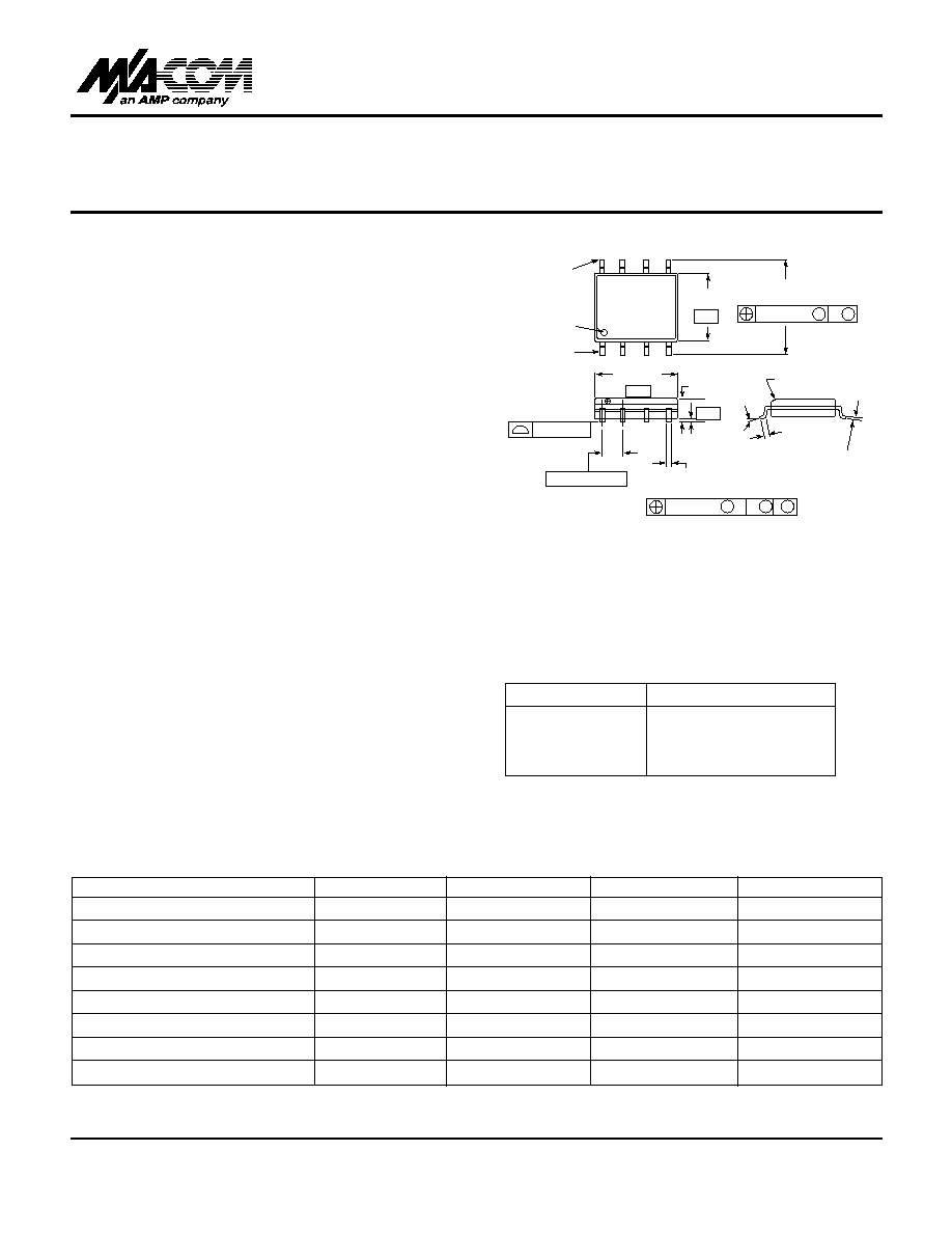
SO-8
0°-8°
.0075-0.0098
(0.19-0.25)
.1890-.1968
(4.80-5.00)
.0099-0.0196
x 45° Chamfer
(0.25-0.50)
.2284-.2440
(5.80-6.20)
PIN 8
Orientation
mark
PIN 1
8- Lead SOP outline dimensions
Narrow body .150
(All dimensions per JEDEC No. MS-012-AA, Issue C)
Dimensions in ( ) are in mm.
.1497-.1574
(3.80-4.00)
- B -
- A -
.050(1.27) BSC.
.013-.020 TYP.
(0.33-0.51)
.0040-.0098
(0.10-0.25)
- C -
.0532-.0688
(1.35-1.75)
.016-.050
(0.40-1.27)
.010(0.25) M B M
.010(0.25) M C A M B S
Unless Otherwise Noted: .xxx = ≠ 0.010 (.xx = ≠ 0.25)
.xx = ≠ 0.02 (.x = ≠0.5)
.004 (0.10)
q
q
q
q
q
q
q
Part Number
Package
MAAM12032
SOIC 8-Lead Plastic
MAAM12032TR
Forward Tape and Reel*
MAAM12032RTR
Reverse Tape and Reel*
MAAM12032SMB
Designer's Kit
Ordering Information
1. See following pages for 3-volt data.
* If specific reel size is required, consult factory for part
number assignment.

Low Noise Amplifier
MAAM12032
M/A-COM, Inc.
s
1011 Pawtucket Boulevard, Lowell, MA 01853 USA
s
Telephone: 800-366-2266
Parameter
Absolute Maximum
V
DD
+10 VDC
Input Power
+17 dBm
Current
2
30 mA
Channel Temperature
3
+150∞C
Operating Temperature
-40∞C to +85∞C
Storage Temperature
-65∞C to +150∞C
Absolute Maximum Ratings
1
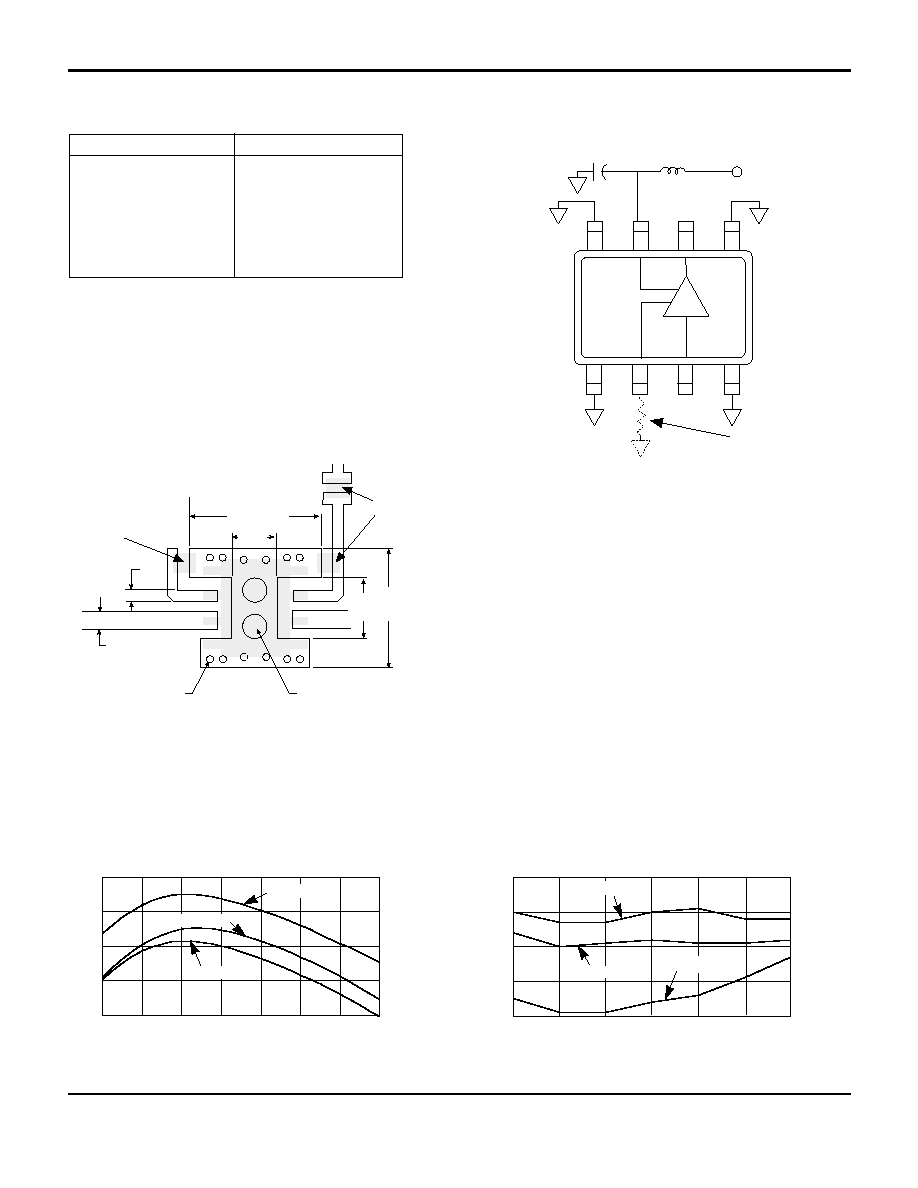
Recommended PCB Configuration
Functional Diagram
1. Operation of this device outside these limits may cause
permanent damage.
2. Only if pin #2 is used to increase current. (See note 6.)
3. Typical thermal resistance ( jc) = +165∞C/W.
RF
OUT
RF
IN
See Note 6
V
DD
500pF
8
7
6
5
1
2
3
4
15 nH
GND
GND
GND
GND
Specifications Subject to Change Without Notice.
V2.00
2.0
1.9
1.8
1.7
1.6
1.70
1.75
1.80
1.85
1.90
1.95
2.00
FREQUENCY (GHz)
NOISE FIGURE (dB)
NOISE FIGURE vs FREQUENCY, T
A
= +25∞C
Notes:
4. Pins 1, 4, 5 and 8 must be RF and DC grounded as shown.
5. Pin 3 is the RF input; pin 6 is the RF output. V
DD
is applied on pin 7.
This pin must be bypassed with a 500-pF surface mount MLC
capacitor, mounted as close as possible to pin 7, and RF decoupled
with a chip inductor having a minimum value of 15 nH (as shown in
the Recommended PCB Configuration).
6. Pin 2 allows use of an external resistor to ground for optional, higher
current bias. For nominal current operation no resistor is used.
For optional 20-mA current operation, connect a 30- to 35-ohm chip
resistor (as shown in the Recommended PCB Configuration).
Typical Performance
17
15
13
11
9
1.5
1.6
1.7
1.8
1.9
2.0
2.1
2.2
FREQUENCY (GHz)
GAIN (dB)
GAIN vs FREQUENCY, T
A
= +25∞C
5 V, 20 mA
5 V, 5 mA
3 V, 5 mA
3 V, 5 mA
5 V, 5 mA
5 V, 20 mA
0.020 (0.51) FR-4 Circuit Board
Dimensions in inches (mm)
.294 (7.47)
.025
(.64)
0.037
(0.94)
R .008
(0.20)
(12 Places)
Plated thru hole
(2 Places)
Plated thru hole
R .025 (0.64)
RF In
See
Note 6
0.245
(6.22)
0.125
(3.18)
RF Out
See
Note 5
V
DD
1
2
3
4
8
7
6
5
0.100
(2.54)

Low Noise Amplifier
MAAM12032
Specifications Subject to Change Without Notice.
V2.00
M/A-COM, Inc.
s
1011 Pawtucket Boulevard, Lowell, MA 01853 USA
s
Telephone: 800-366-2266
3.0
2.5
2.0
1.5
1.0
1.5
1.6
1.7
1.8
1.9
2.0
2.1
2.2
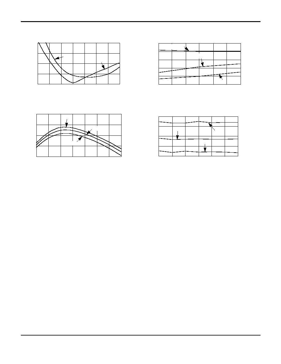
VSWR
FREQUENCY (GHz)
VSWR
VS
FREQUENCY @ 5 V, 5 mA, T
A
= +25∞C
6
4
2
0
-2
-4
1.70
1.75
1.80
1.85
1.90
1.95
2.00
FREQUENCY (GHz)
INPUT IP
3
(dBm)
INPUT IP3 vs FREQUENCY, T
A
= +25∞C
17
15
13
11
9
1.5
1.6
1.7
1.8
1.9
2.0
2.1
2.2
FREQUENCY (GHz)
GAIN
(dB)
GAIN vs FREQUENCY @ 5 V, 5 mA
2.5
2.2
1.9
1.6
1.3
1.70
1.75
1.80
1.85
1.90
1.95
2.00
FREQUENCY (GHz)
NOISE FIGURE (dB)
NOISE FIGURE vs FREQUENCY @ 5 V, 5 mA
Input
Output
3 V, 5 mA
-40∞C
+25∞C
+85∞C
+25∞C
-40∞C
+85∞C
5 V, 20mA
5 V, 5 mA
Additional information is available in Application Note M540,
"M/A-COM GaAs MMIC LNA SOIC-8 Platform."
