0.5W X/Ku-Band Power Amplifier
8.0-12.5 GHz
MAAPGM0034-DIE
8.0-12.5 GHz GaAs MMIC Amplifier
RO-P-DS-3019 - -
Preliminary Information
Features
8.0-12.5 GHz Operation
0.5 Watt Saturated Output Power Level
Variable Drain Voltage (4-10V) Operation
Self-Aligned MSAG
Æ
MESFET Process
Primary Applications
Point-to-Point Radio
Weather Radar
Description
The
MAAPGM0034-Die
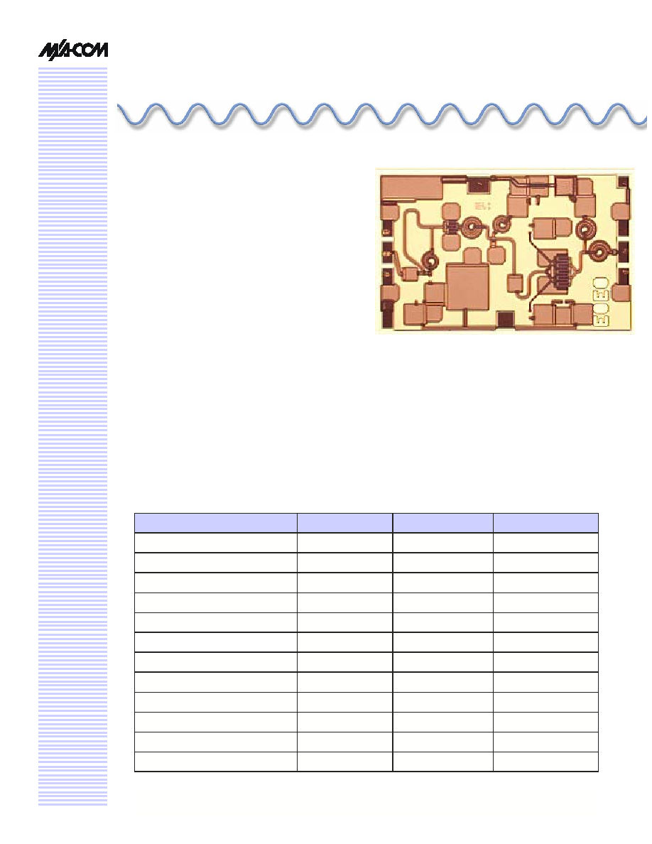
is a 2-stage 0.5 W power amplifier
with on-chip bias networks. This product is fully matched to
50 ohms on both the input and output. It can be used as a
power amplifier stage or as a driver stage in high power
applications.
Each device is 100% RF tested on wafer to ensure
performance compliance. The part is fabricated using M/A-
COM's repeatable, high performance and highly reliable
GaAs Multifunction Self-Aligned Gate (MSAG
Æ
) MESFET
Process. This process features silicon nitride passivation
and polyimide scratch protection.
Electrical Characteristics: T
B
= 40∞C
1
, Z
0
= 50
, V
DD
= 10V, V
GG
= -2V, P
in
= 18 dBm
Parameter
Typical
Units
Bandwidth
8.0-12.5
GHz
1-dB Compression Point
26
dBm
Small Signal Gain
15
dB
Input VSWR
2:1
Gate Current
< 2
mA
Drain Current
< 200
mA
Power Added Efficiency
35
%
Output Power
28
dBm
Output Third Order Intercept
33
dBm
Noise Figure
8
dB
2
nd
Harmonic
-28
dBc
Symbol
f
P
OUT
PAE
P1dB
G
Input VSWR
I
GG
I
DD
OTOI
NF
2f
3
rd
Harmonic
3f
-35
dBc
1. T
B
= MMIC Base Temperature

0.5W X/Ku-Band Power Amplifier
MAAPGM0034-DIE
RO-P-DS-3019 - - 2/6
Specifications subject to change without notice.
Customer Service: Tel. (888)-563-3949
Email: macom_adbu_ics@tycoelectronics.com
North America: Tel. (800) 366-2266
Asia/Pacific: Tel.+81-44-844-8296, Fax +81-44-844-8298
Europe: Tel. +44 (1344) 869 595, Fax+44 (1344) 300 020
Visit www.macom.com for additional data sheets and product information.
Maximum Operating Conditions
1
Operating Instructions
This device is static sensitive. Please handle with
care. To operate the device, follow these steps.
1. Apply V
GG
= -2 V, V
DD
= 0 V.
2. Ramp V
DD
to desired voltage, typically 10.0 V.
3. Adjust
V
GG
to set I
DQ
, (approximately @ ≠2 V).
4. Set RF input.
5.
Power down sequence in reverse. Turn gate
voltage off last.
Recommended Operating Conditions
Parameter
Symbol
Absolute Maximum
Units
Input Power
P
IN
21.0
dBm
Drain Supply Voltage
V
DD
+12.0
V
Gate Supply Voltage
V
GG
-3.0
V
Quiescent Drain Current (No RF)
I
DQ
190
mA
Quiescent DC Power Dissipated (No RF)
P
DISS
1.2
W
Junction Temperature
T
J
180
∞C
Storage Temperature
T
STG
-55 to +150
∞C
1. Operation outside of these ranges may reduce product reliability. Operation at other than the typical values may
result in performance outside the guaranteed limits.
2. Maximum MMIC Base Temperature = 150∞C --64.1 ∞C/W * V
DD
* I
DQ
Characteristic
Symbol
Min
Typ
Max
Unit
Drain Voltage
V
DD
4.0 10.0 10.0 V
Gate Voltage
V
GG
-2.3 -2.0 -1.5
V
Input Power
P
IN
18.0
19.0
dBm
Junction Temperature
T
J
150
∞C
MMIC Base Temperature
T
B
Note 2
∞C

0.5W X/Ku-Band Power Amplifier
MAAPGM0034-DIE
RO-P-DS-3019 - - 3/6
Specifications subject to change without notice.
Customer Service: Tel. (888)-563-3949
Email: macom_adbu_ics@tycoelectronics.com
North America: Tel. (800) 366-2266
Asia/Pacific: Tel.+81-44-844-8296, Fax +81-44-844-8298
Europe: Tel. +44 (1344) 869 595, Fax+44 (1344) 300 020
Visit www.macom.com for additional data sheets and product information.
Figure 1. Output Power and Power Added Efficiency vs. Frequency at V
DD
= 10V
and P
in
= 18 dBm.
0
10
20
30
40
50
7.5
8.0
8.5
9.0
9.5
10.0
10.5
11.0
11.5
12.0
12.5
13.0
Frequency (GHz)
0
10
20
30
40
50
POUT
PAE
0
10
20
30
40
50
4
5
6
7
8
9
10
Drain Voltage (V)
0
10
20
30
40
50
POUT
PAE
Figure 2. Saturated Output Power and Power Added Efficiency vs. Drain Voltage at f
o
= 10 GHz.

0.5W X/Ku-Band Power Amplifier
MAAPGM0034-DIE
RO-P-DS-3019 - - 4/6
Specifications subject to change without notice.
Customer Service: Tel. (888)-563-3949
Email: macom_adbu_ics@tycoelectronics.com
North America: Tel. (800) 366-2266
Asia/Pacific: Tel.+81-44-844-8296, Fax +81-44-844-8298
Europe: Tel. +44 (1344) 869 595, Fax+44 (1344) 300 020
Visit www.macom.com for additional data sheets and product information.
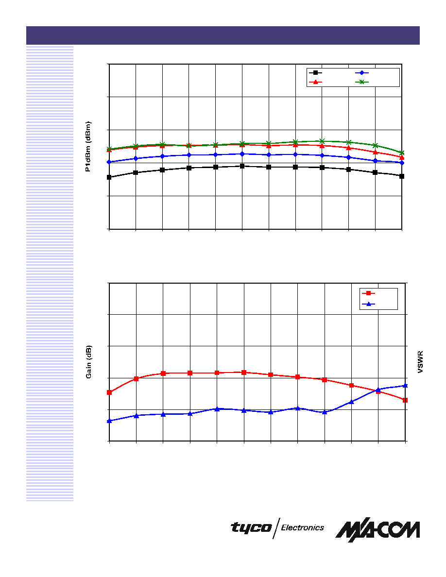
Figure 3. 1dB Compression Point vs. Drain Voltage
0
10
20
30
40
50
7.5
8.0
8.5
9.0
9.5
10.0
10.5
11.0
11.5
12.0
12.5
13.0
Frequency (GHz)
VDD = 4
VDD = 6
VDD = 8
VDD = 10
Figure 4. Small Signal Gain and Input VSWR vs. Frequency at V
DD
= 10V.
5
10
15
20
25
30
7.5
8.0
8.5
9.0
9.5
10.0
10.5
11.0
11.5
12.0
12.5
13.0
Frequency (GHz)
1
2
3
4
5
6
GAIN
VSWR

0.5W X/Ku-Band Power Amplifier
MAAPGM0034-DIE
RO-P-DS-3019 - - 5/6
Specifications subject to change without notice.
Customer Service: Tel. (888)-563-3949
Email: macom_adbu_ics@tycoelectronics.com
North America: Tel. (800) 366-2266
Asia/Pacific: Tel.+81-44-844-8296, Fax +81-44-844-8298
Europe: Tel. +44 (1344) 869 595, Fax+44 (1344) 300 020
Visit www.macom.com for additional data sheets and product information.
Mechanical Information
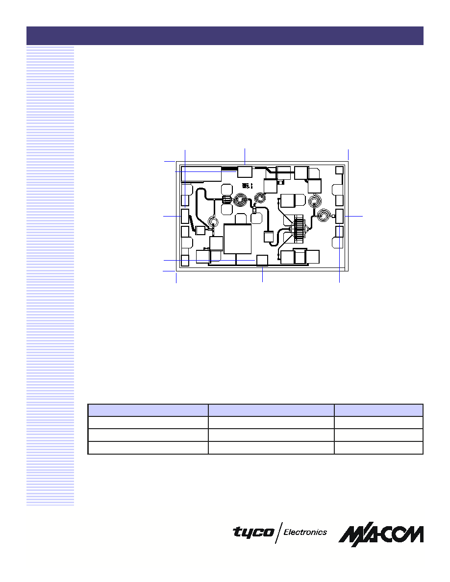
Chip Size: 2.480 x 1.580 x 0.075 mm
(
98 x 62 x 3 mils)
Pad
Size (
µm)
RF In and Out
100 x 200
DC Drain Supply Voltage VDD
200 x 150
DC Gate Supply Voltage VGG
150 x 150
Size (mils)
4 x 8
8 x 6
6 x 6
Bond Pad Dimensions
Chip edge to bond pad dimensions are shown to the center of the bond pad.
V
DD
V
GG
IN
OU
T
0.152 mm.
0.790 mm.
1.428 mm.
1.580 mm.
0.790 mm.
1.240 mm.
0.127 mm
.
0.990 mm
.
2.480 mm
.
0
0
2.353 mm
.
Figure 5. Die Layout
