MAAPGM0035
2.5-5.5 GHz GaAs MMIC Amplifier
RO-P-DS-3071
Preliminary Information
Features
2.5-5.5 GHz Operation
1.6 Watt Saturated Output Power Level
Variable Drain Voltage (4-10V) Operation
Self-Aligned MSAG
Æ
MESFET Process
High Performance Ceramic Bolt Down Package
Primary Applications
WLL
MMDS
SatCom
Description
The
MAAPGM0035
is a packaged, 2-stage, 1.6 W power
amplifier with on-chip bias networks in a bolt down ceramic
package, allowing easy assembly. This product is fully
matched to 50 ohms on both the input and output. It can be
used as a power amplifier stage or as a driver stage in high
power applications.
Each device is 100% RF tested to ensure performance
compliance. The part is fabricated using M/A-COM's GaAs
Multifunction Self-Aligned Gate (MSAG
Æ
) MESFET
Process.
Parameter
Symbol
Absolute Maximum
Units
Input Power
P
IN
25.0
dBm
Drain Supply Voltage
V
DD
+12.0
V
Gate Supply Voltage
V
GG
-3.0
V
Quiescent Drain Current (No RF)
I
DQ
790
mA
Junction Temperature
T
J
180
∞C
Storage Temperature
T
STG
-55 to +150
∞C
Quiescent DC Power Dissipated (No RF)
P
DISS
6.3
W
Maximum Operating Conditions
1
1. Operation outside of these ranges may reduce product reliability.
APGM0035
YWWLLLL
1.6W S/C-Band Power Amplifier
2.5-5.5 GHz
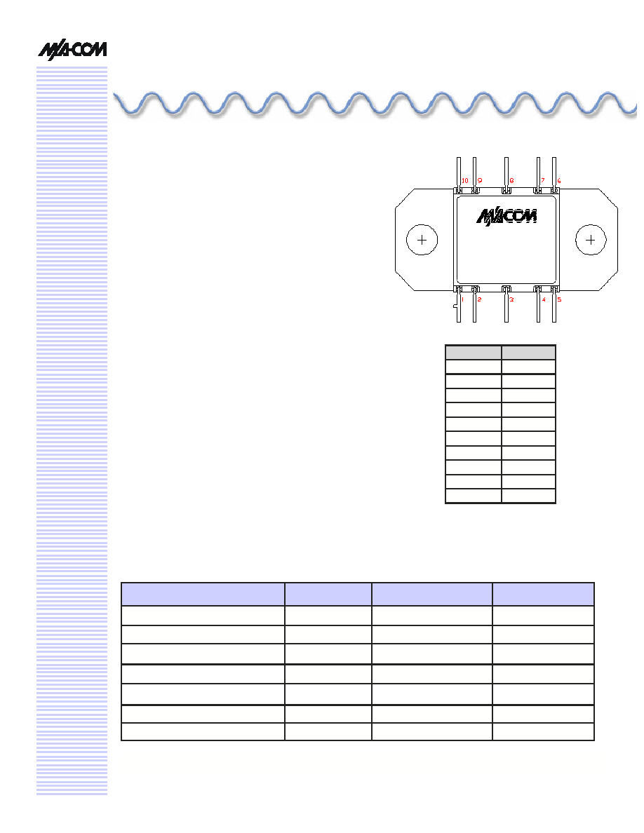
Pin Number
Description
1
No Connection
2
V
GG
3
RF IN
4
V
GG
5
No Connection
9
V
DD
6
No Connection
10
No Connection
8
RF OUT
7
V
DD

RO-P-DS-3071
2/6
1.6W S/C-Band Power Amplifier
MAAPGM0035
V 1.00
Specifications subject to change without notice.
Email: macom_adbu_ics@tycoelectronics.com
n
North America: Tel. (800) 366-2266
n
Asia/Pacific: Tel.+81-44-844-8296, Fax +81-44-844-8298
n
Europe: Tel. +44 (1908) 574 200, Fax+44 (1908) 574 300
Visit www.macom.com for additional data sheets and product information.
Parameter
Symbol
Typical
Units
Bandwidth
f
2.5-5.5
GHz
Output Power
POUT
32
dBm
Power Added Efficiency
PAE
32
%
1-dB Compression Point
P1dB
32
dBm
Small Signal Gain
G
17
dB
Input VSWR
VSWR
1.5:1
Output VSWR
VSWR
3:1
Gate Supply Current
I
GG
< 6
mA
Drain Supply Current
I
DD
< 850
mA
Noise Figure
NF
7
dB
2
nd
Harmonic
2f
-10
dBc
3
rd
Harmonic
3f
-20
dBc
3
rd
Order Intermodulation Distortion,
Single Carrier Level = 22 dBm
IM3
-16
dBm
5
th
Order Intermodulation Distortion,
Single Carrier Level = 22 dBm
IM5
-47
dBm
Output Third Order Intercept
OTOI
42
dBm
Electrical Characteristics: T
B
= 40∞C
3
, Z
0
= 50
, V
DD
= 8V, V
GG
= -1.8V, P
in
= 20 dBm, R
G
= 121O
Operating Instructions
This device is static sensitive. Please handle with care. To operate the device,
follow these steps.
1. Apply V
GG
= -2.0 V, V
DD
= 0 V.
2. Ramp V
DD
to desired voltage, typically 8 V.
3. Adjust
V
GG
to set I
DQ
, (approxmately @ ≠1.8V).
4. Set RF input.
5.
Power down sequence in reverse. Turn V
GG
off last.
Characteristic
Symbol
Min
Typ
Max
Unit
Drain Supply Voltage
V
DD
4.0
8.0
10.0
V
Gate Supply Voltage
V
GG
-2.3
-2.0
-1.5
V
Input Power
P
IN
20.0
23.0
dBm
Junction Temperature
T
J
150
∞C
MMIC Base Temperature
T
B
Note 2
∞C
Thermal Resistance
T
JC
14.9
∞C/W
Recommended Operating Conditions
2. Maximum MMIC Base Temperature = 150∞C -- T
JC
* V
DD
* I
DQ
3. T
B
= MMIC Base Temperature

RO-P-DS-3071
3/6
1.6W S/C-Band Power Amplifier
MAAPGM0035
V 1.00
Specifications subject to change without notice.
Email: macom_adbu_ics@tycoelectronics.com
n
North America: Tel. (800) 366-2266
n
Asia/Pacific: Tel.+81-44-844-8296, Fax +81-44-844-8298
n
Europe: Tel. +44 (1908) 574 200, Fax+44 (1908) 574 300
Visit www.macom.com for additional data sheets and product information.
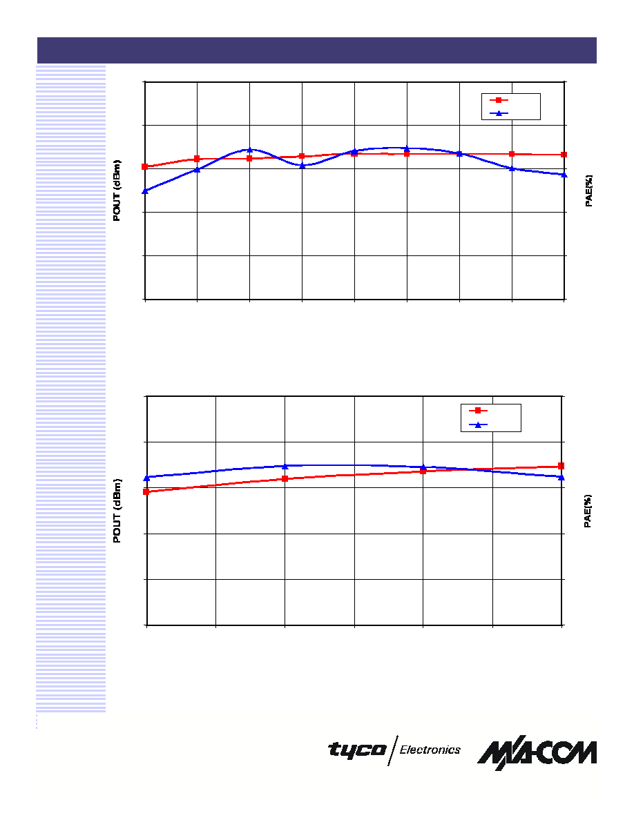
Figure 1. Output Power and Power Added Efficiency vs. Frequency
at V
DD
= 8V and Pin = 20 dBm.
0
10
20
30
40
50
2.0
2.5
3.0
3.5
4.0
4.5
5.0
5.5
6.0
Frequency (GHz)
0
10
20
30
40
50
POUT
PAE
0
10
20
30
40
50
4
5
6
7
8
9
10
Drain Voltage (volts)
0
10
20
30
40
50
POUT
PAE
Figure 2. Saturated Output Power and Power Added Efficiency vs. Drain Voltage at f
o
= 4 GHz.

RO-P-DS-3071
4/6
1.6W S/C-Band Power Amplifier
MAAPGM0035
V 1.00
Specifications subject to change without notice.
Email: macom_adbu_ics@tycoelectronics.com
n
North America: Tel. (800) 366-2266
n
Asia/Pacific: Tel.+81-44-844-8296, Fax +81-44-844-8298
n
Europe: Tel. +44 (1908) 574 200, Fax+44 (1908) 574 300
Visit www.macom.com for additional data sheets and product information.
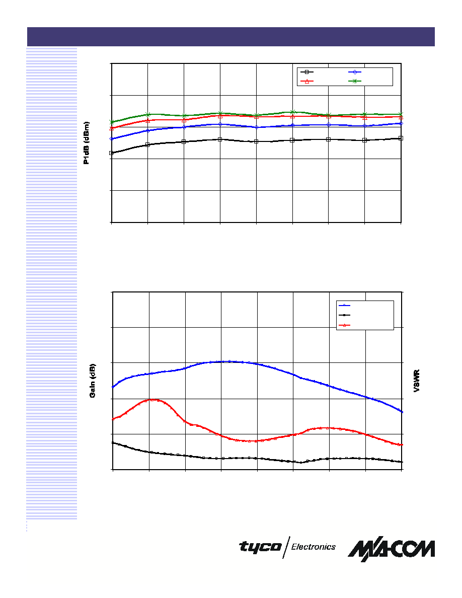
Figure 3. 1dB Compression Point vs. Drain Voltage
0
10
20
30
40
50
2.0
2.5
3.0
3.5
4.0
4.5
5.0
5.5
6.0
Frequency (GHz)
VDD = 4
VDD = 6
VDD = 8
VDD = 10
5
10
15
20
25
30
2.0
2.5
3.0
3.5
4.0
4.5
5.0
5.5
6.0
Frequency (GHz)
1
2
3
4
5
6
Gain
Input VSWR
Output VSWR
Figure 4. Small Signal Gain and VSWR vs. Frequency at VDD = 8V.

RO-P-DS-3071
5/6
1.6W S/C-Band Power Amplifier
MAAPGM0035
V 1.00
Specifications subject to change without notice.
Email: macom_adbu_ics@tycoelectronics.com
n
North America: Tel. (800) 366-2266
n
Asia/Pacific: Tel.+81-44-844-8296, Fax +81-44-844-8298
n
Europe: Tel. +44 (1908) 574 200, Fax+44 (1908) 574 300
Visit www.macom.com for additional data sheets and product information.
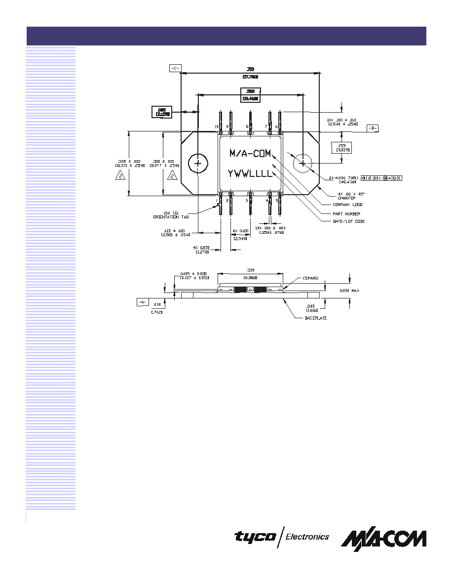
Figure 5. CR-15 Package Dimensions
The CR-15 is a high frequency, low thermal resistance package. The package consists of a cofired
ceramic construction with a copper-tungsten base and iron-nickel-cobalt leads. The finish consists of
electrolytic gold over nickel plate.
APGM0035

RO-P-DS-3071
6/6
1.6W S/C-Band Power Amplifier
MAAPGM0035
V 1.00
Specifications subject to change without notice.
Email: macom_adbu_ics@tycoelectronics.com
n
North America: Tel. (800) 366-2266
n
Asia/Pacific: Tel.+81-44-844-8296, Fax +81-44-844-8298
n
Europe: Tel. +44 (1908) 574 200, Fax+44 (1908) 574 300
Visit www.macom.com for additional data sheets and product information.
Assembly Instructions:
This flange mount style package provides a robust interface between a highly integrated GaAs MMIC device and a circuit board
which may be assembled using conventional surface mount techniques. A thin shim made of a thermally and electrically
conductive, ductile material should be used prior to installation of the CR-15 to improve the thermal and electrical performance of
the package to housing interface. Refer to M/A-COM Application Note #M567* for more information .
For applications where surface mount components are to be installed after the CR-15 installation, this package will not be
damaged when subjected to typical convection or IR oven reflow profiles. Refer to M/A-COM Application Note #M538* for
maximum allowable reflow time and temperature. Alternatively, the package leads may be individually soldered. Whether an iron
or hot gas soldering equipment is used, care should be taken to insure that the temperature is well controlled and electric static
discharge (ESD) safe.
Biasing Note: Must apply negative bias to V
GG
before applying positive bias to V
DD
to prevent
damage to amplifier.
* Application Notes can be found by going to the Site Search Page on M/A-COM's web page
(http://www.macom.com/search/search.jsp) and searching for the required Application Note.
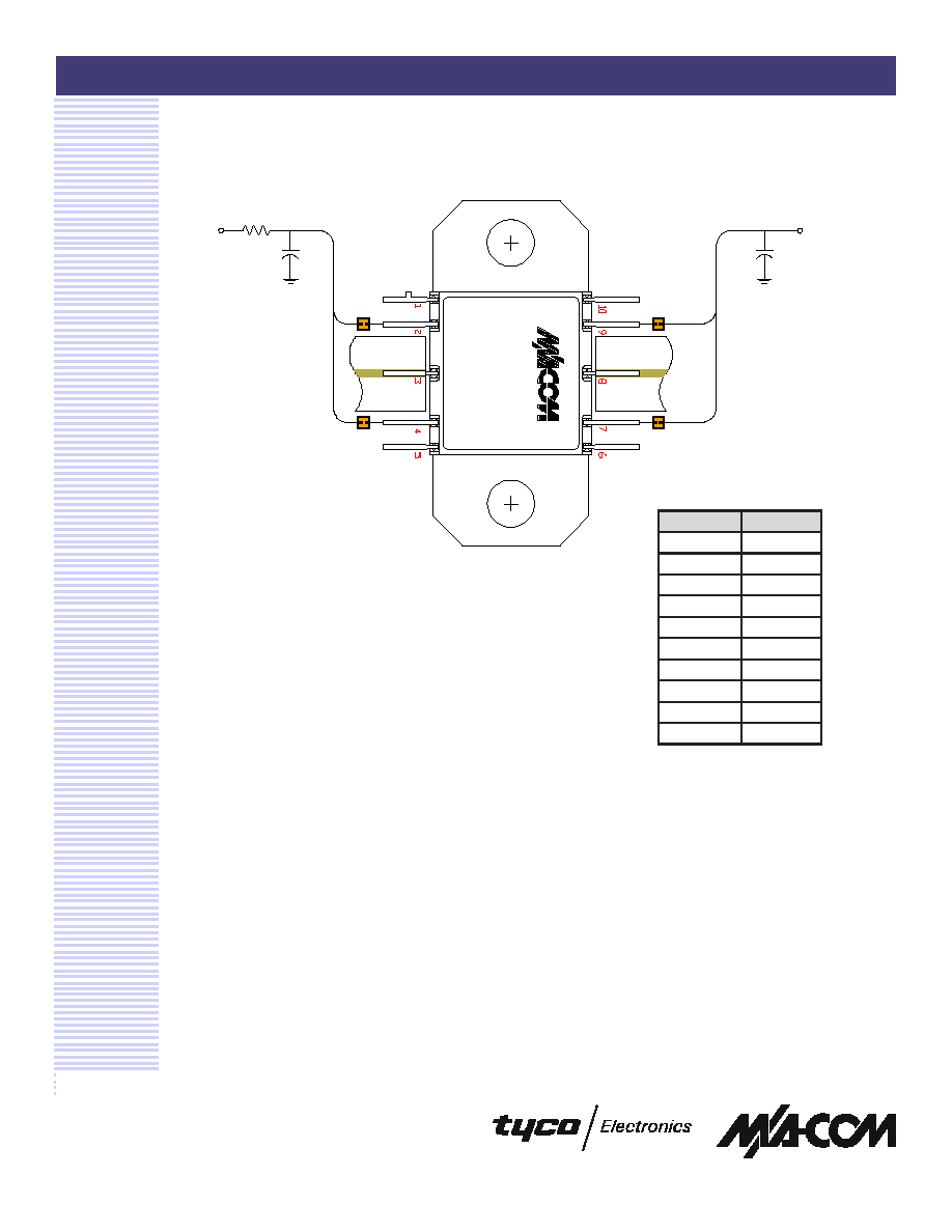
Figure 6. Recommended Bias Configuration
APGM0035
YWWLLLL
121 O
Pin Number
Description
1
No Connection
2
V
GG
3
RF IN
4
V
GG
5
No Connection
9
V
DD
6
No Connection
10
No Connection
8
RF OUT
7
V
DD
RF
OUT
RF
IN
0.1
µ
F
V
GG
0.1
µ
F
V
DD
100 pF
100 pF
100 pF
100 pF
