North America: Tel. (800) 366-2266, Fax (800) 618-8883
Asia/Pacific: Tel.+81-44-844-8296, Fax +81-44-844-8298
Europe: Tel. +44 (1344) 869 595, Fax+44 (1344) 300 020
Specifications subject to change without notice.
Visit www.macom.com for additional data sheets and product information.
V 1.0
VC
C1
GND
GND
GND
RFIN
GND
GND
GND
RFOUT
RFOUT
GND
GND
VC
C1
VC
C2
GND
VPD
1
VMO
D
E
VPD
2
GN
D
BIA
S
GN
D
1
20
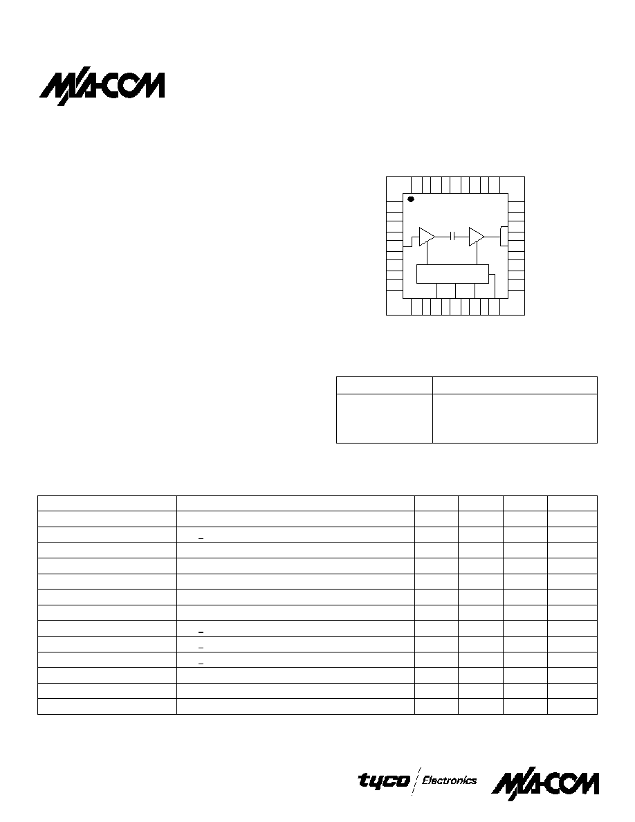
Bias Network
Functional Block Diagram
Ordering Information
Part Number
Package
MAAPSS0003
FQFP-N 4.0mm Plastic Package
MAAPSS0003TR
Forward Tape and Reel
1
MAAPSS0003RTR
Reverse Tape and Reel
1
1. If specific reel size is required, consult factory for part number
assignment.
Features
�
High Gain 2-stage HBT Amplifier
�
Single Supply, 3V Operation
�
29dBm Linear Output Power
�
High Efficiency
�
Low Quiescent Current
�
Operates in US and Korean PCS Bands
�
Miniature FQFP-N 4mm Plastic Package
Description
M/A-COM's MAAPSS0003 is a high power, high efficiency
linear power amplifier in a miniature FQFP-N 4mm plastic
package. The MAAPSS0003 includes a 2-stage amplifier and
bias control network. Analog signals control output power and
power-off for active and standby modes.
The MAAPSS0003 is ideally suited for TDMA and CDMA
handset applications where high linearity and low power
consumption are important transmitter requirements. The
MAAPSS0003 is design to operate with the MD59-0062
Upconverter/Driver IC.
The MAAPSS0003 is fabricated using M/A-COM's iHBT
HBT process. The process utilizes the InGaP/GaAs materials
system for reduced performance variation over temperature,
high reliability and improved manufacturability.
MAAPSS0003
PCS TDMA/CDMA Power Amplifier
1750 - 1910 MHz
1
Parameter
Test Conditions
Units
Min.
Typ.
Max.
Frequency Range
MHz
1850
1910
Small Signal Gain
P
OUT
< 0 d:Bm
dB
27
Linear Output Power
At maximum ACPR Level
dBm
29
ACPR
1
dBc
-44
Efficiency
P
OUT
= 29 dBm
%
32
Quiescent Current
mA
100
Noise Power in Rx Band
P
OUT
< 29 dBm
dBm/Hz
-139
2
nd
Harmonic Suppression
P
OUT
< 29 dBm
dBc
-40
3
rd
Harmonic Suppression
P
OUT
< 29 dBm
dBc
-40
Input V
SWR
2:1
Stability
No oscillations, any phase
5:a
Output Load Ruggedness V
SWR
No damage, any phase
10:1
Linear Gain
P
OUT
= 29 dBm
dB
26
Electrical Specifications: V
CC
= 3.4V, Vref = 3.0V, T
A
= +25�C
Preliminary
1. Per IS95: ACPR is defined as the ratio of the total power in a 1.228MHz bandwidth to the power within a 30KHz bandwidth measured at
�
1.25MHz
offset from the carrier frequency.

North America: Tel. (800) 366-2266, Fax (800) 618-8883
Asia/Pacific: Tel.+81-44-844-8296, Fax +81-44-844-8298
Europe: Tel. +44 (1344) 869 595, Fax+44 (1344) 300 020
Specifications subject to change without notice.
Visit www.macom.com for additional data sheets and product information.
V 1.0
PCS TDMA/CDMA Power Amplifier, 1750 - 1910 MHz
MAAPSS0003
2
PIN #
PIN Name
Description
1
GND
DC and RF Ground
2
GND
DC and RF Ground
3
RFIN
RF input to the amplifier, requires matching
network
4
GND
DC and RF Ground
5
GND
DC and RF Ground
6
GND
DC and RF Ground
7
VPD1
1
st
stage bias control
8
VMODE
High / Low gain selector
9
VPD2
2
nd
stage bias control
10
BIAS GND
Bias Control Ground, requires RF choke
11
GND
DC and RF Ground
12
GND
DC and RF Ground
13
RF OUT
RF Output of the amplifier, requires
matching network
14
RF OUT
RF Output of the amplifier, requires
matching network
15
GND
DC and RF Ground
16
GND
DC and RF Ground
17
V
CC2
Voltage supply for the bias network
18
GND
DC and RF Ground
19
V
CC1
Voltage supply for 1
st
stage, requires
matching network
20
V
CC1
Voltage supply for 1
st
stage, requires
matching network
PIN Configuration
VCC1
GND
GND
GND
RFIN
GND
GND
GND
RFOUT
RFOUT
GND
GND
VCC
1
VCC
2
GND
VP
D1
VM
OD
E
VP
D2
GN
D
BI
A
S
GND
1
20
Bias Network
Block Diagram
E2
20 x b
e
4 x e
L
e
4 x e
D2
D
E
E1
D1
A
A2
A1
A3
FQFP-N 4 mm
Measurement (mm)
Min.
Nom.
Max.
A
0.80
0.90
1.00
A1
0
0.02
0.05
A2
0
0.65
1.00
A3
0.25 ref.
b
0.18
0.23
0.30
D
4.00 basic
D1
3.75 basic
D2
0.75
1.70
2.25
e
0.50 basic
E
4.00 basic
E1
3.75 basic
E2
0.75
1.70
2.25
L
0.35
0.55
0.75
Dim.

North America: Tel. (800) 366-2266, Fax (800) 618-8883
Asia/Pacific: Tel.+81-44-844-8296, Fax +81-44-844-8298
Europe: Tel. +44 (1344) 869 595, Fax+44 (1344) 300 020
Specifications subject to change without notice.
Visit www.macom.com for additional data sheets and product information.
V 1.0
RF IN
R1
C2
C6
C7
VCC
C1
C4
C3
C5
R2
R3
T1
T2
T3
VPD VMODE
L1
L2
C8
C9
C10
L3
1
20
Bias Network
RF OUT
3
PCS TDMA/CDMA Power Amplifier, 1750 - 1910 MHz
MAAPSS0003
Sample Board Schematic
Ref. Designation
Value
Purpose
C1
3.0 pF
RF Matching / DC Block
C2
2.7 pF
RF Matching
C3, C7
4.7 pF
RF Matching
C4
2.2 pF
RF Matching
C5
15 pF
DC Block
C8, C9
15 pF
RF Matching
C6
0.8 pF
RF Matching
C10
9.0 pF
RF Matching
L1, L2
15.0 nH
RF Choke
L3
8.2 nH
RF Choke
R1
TBD
Bias Adjust
R2
TBD
Bias Adjust
R3
TBD
Bias Adjust
T1
350 Mils
RF Matching
T2
40 Mils
RF Matching
T3
250 Mils
RF Matching
External Circuitry Parts List
1
1. Values of external elements not final.


