PCS LNA/Downconverter,
1800 - 2000 MHz
MADCSM0012
V 1.00
Features
n
Highly Integrated LNA and Downconverter
n
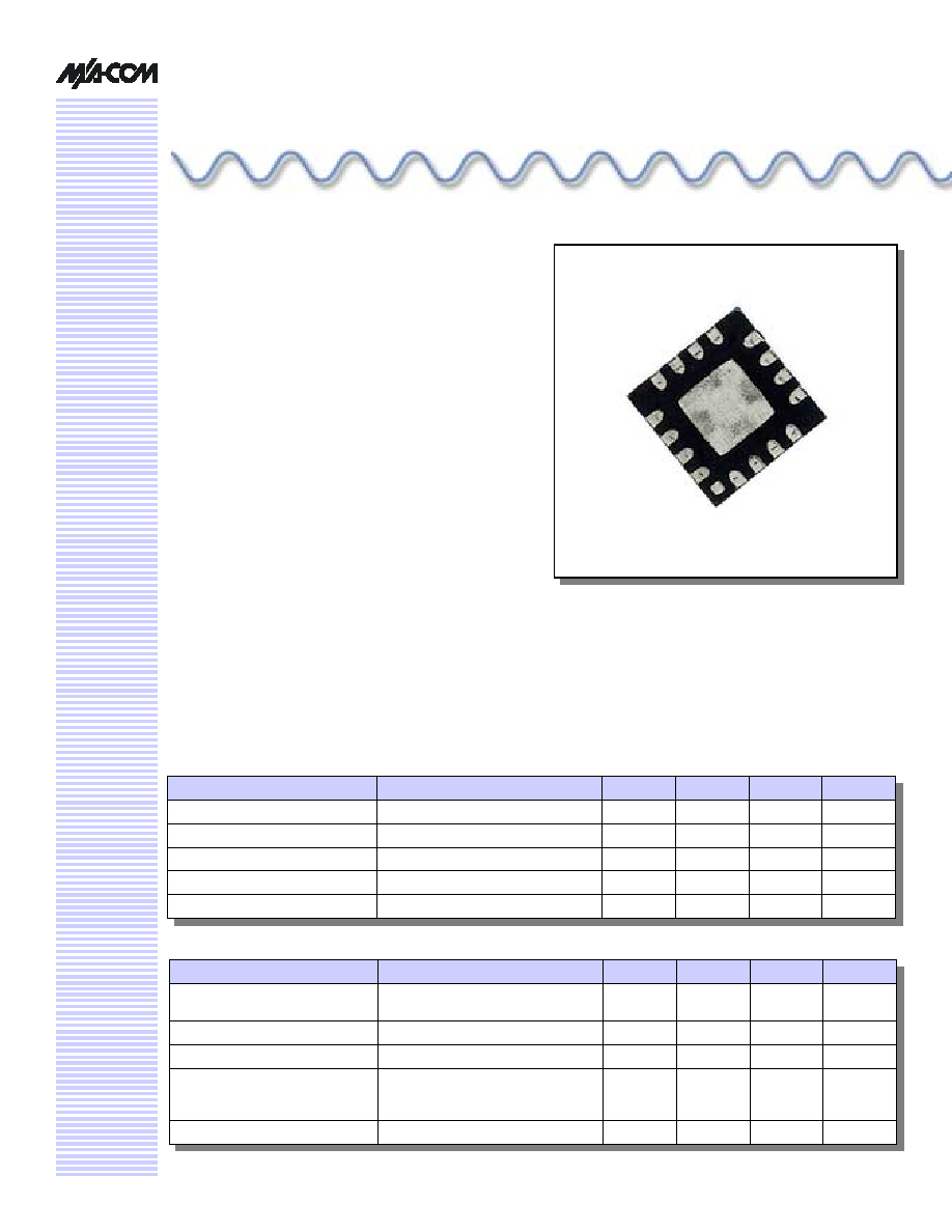
3mm FQFP-N Plastic Package
n
Operates Over 2.7 V to 5 V Supply Voltage
n
Low Noise Figure: 2.3 dB Typical
n
High Input Intercept Point: -9 dBm Typical
n
Continuous Current Control Downconverter
n
Low LO Drive Level: ≠10 dBm
Description
M/A-COM's MADCSM0012 integrated downconverter
combines a low noise amplifier, a RF amplifier, a
downconverting mixer, an IF amplifier and LO buffer
amplifier. The MADCSM0012 is packaged in a low cost
3mm FQFP-N plastic package with an exposed pad for
improved high frequency grounding.
M/A-COM designed the MADCSM0012 for handsets
requiring wide dynamic range and low power consumption.
By application of a suitable control voltage to pin 6, the
linearity of the device can be controlled in real time to keep
the current as low as possible.
The MADCSM0012 is fabricated using M/A-COM's
0.5-micron low noise E/D GaAs MESFET process. The
process features full passivation for increased performance
and reliability.
Electrical Specifications - Korean Band PCS:
Test Conditions: VDD = 3.0 V,
RF = 1855 MHz, IF = 210 MHz, LO = 1645 MHz, LO = -10 dBm, T
A
= 25∞C
Parameter
Test Conditions
Units
Min
Typ
Max
Gain
--
dB
--
15
--
Noise Figure
--
dB
--
1.35
--
VSWR In/Out
--
Ratio
--
2:1
--
Input IP3
--
dBm
--
6
--
Idd
--
mA
--
15
--
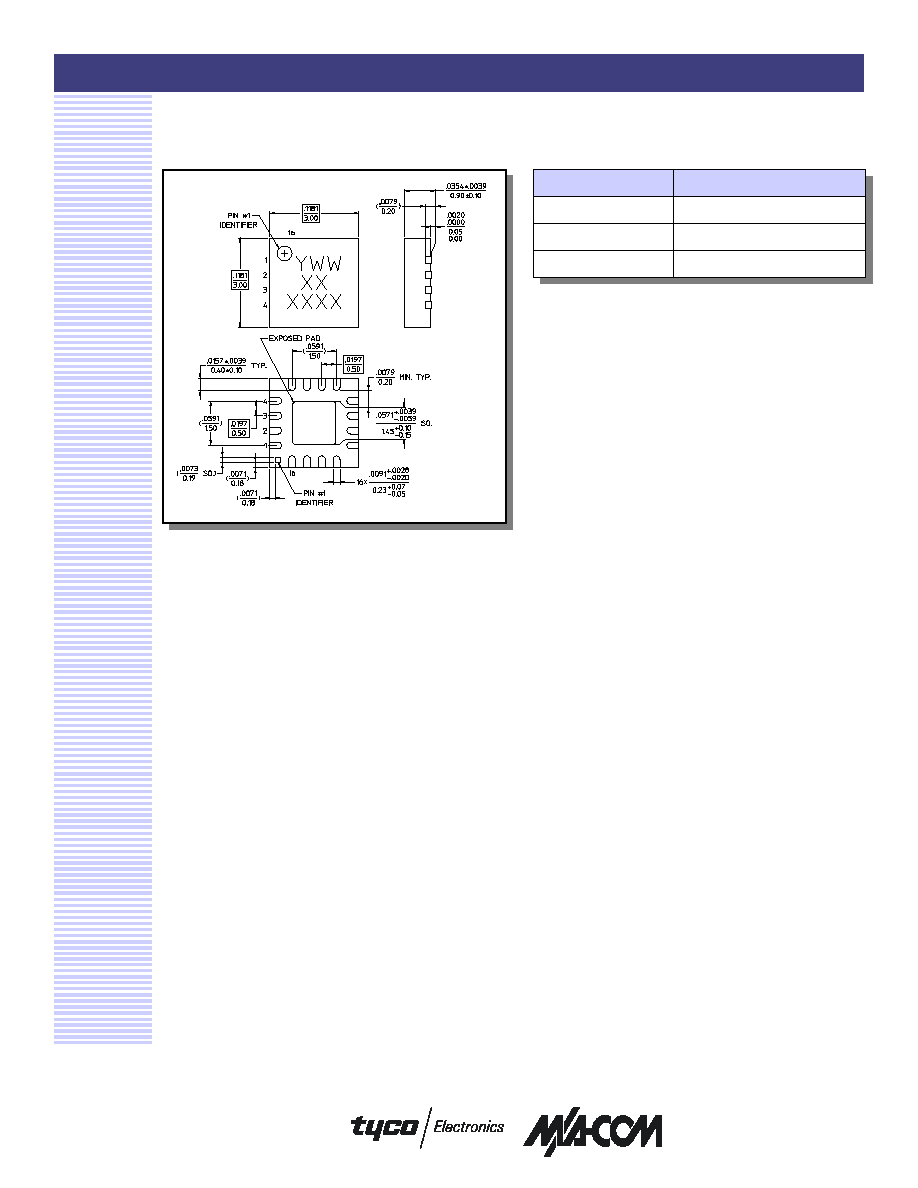
FQFP-N, 3mm, 16 Lead
Low Noise Amplifier
Parameter
Test Conditions
Units
Min
Typ
Max
Conversion Gain
V
CTL
= 3.0 V
V
CTL
= 1.0 V
dB
dB
22.5
--
25
21
27.5
--
Noise Figure
V
CTL
= 3.0 V
dB
--
2.3
3.2
Input IP3
RF Input = -30 dBm, V
CTL
= 3.0V
dBm
-11
-9
--
Isolation
LO to RF, V
CTL
= 3.0 V
LO to IF, V
CTL
= 3.0 V
RF to IF, V
CTL
= 3.0 V
dB
dB
dB
--
--
--
50
31
18
--
--
--
Idd
V
CTL
= 3.0 V
mA
--
25
37
Cascaded LNA/Downconverter
1
1. Complete cascaded measurements taken with 3 dB pad between LNA output and Downconverter input (RFA IN).

PCS LNA/Downconverter, 1800 - 2000 MHz
MADCSM0012
V 1.00
M/A-COM Inc. and its affiliates reserve the right to make changes to the product(s)
or information contained herein without notice.
Visit www.macom.com for additional data sheets and product information.
n
North America: Tel. (800) 366-2266
n
Asia/Pacific: Tel.+81-44-844-8296, Fax +81-44-844-8298
n
Europe: Tel. +44 (1344) 869 595, Fax+44 (1344) 300 020
2
Pin Configuration
Pin
No.
Pin
Name
Description
1
LNA IN
Input to LNA; RF matching required
2
GND
DC and RF Ground
3
LNA SRC
Source of LNA output stage FET.
RF bypassing required. Off-chip resistor
may be used to increase IIP3
4
LNA OUT
50 Ohm LNA output; DC Blocked
5
LNA V
DD2
LNA second stage supply voltage;
RF bypassing required
6
V
CTL
Downconverter bias control.
0 to 3.0 V allowed
7
GND
DC and RF Ground
8
RFA V
DD
RFA supply voltage;
RF bypassing required
9
GND
DC and RF Ground
10
RFA IN
50 Ohm RFA Input; DC Blocked
11
LOA V
DD
LOA supply voltage;
RF bypassing required
12
GND
DC and RF Ground
13
LOA IN
Local oscillator input (-10 to ≠5 dBm)
14
IF OUT
IF Output of downconverter;
IF matching required
15
IFA
MATCH
IF matching between mixer and IFA;
required an inductor to ground
16
LNA V
DD1
LNA first stage supply voltage;
RF bypassing required
Absolute Maximum Ratings
2
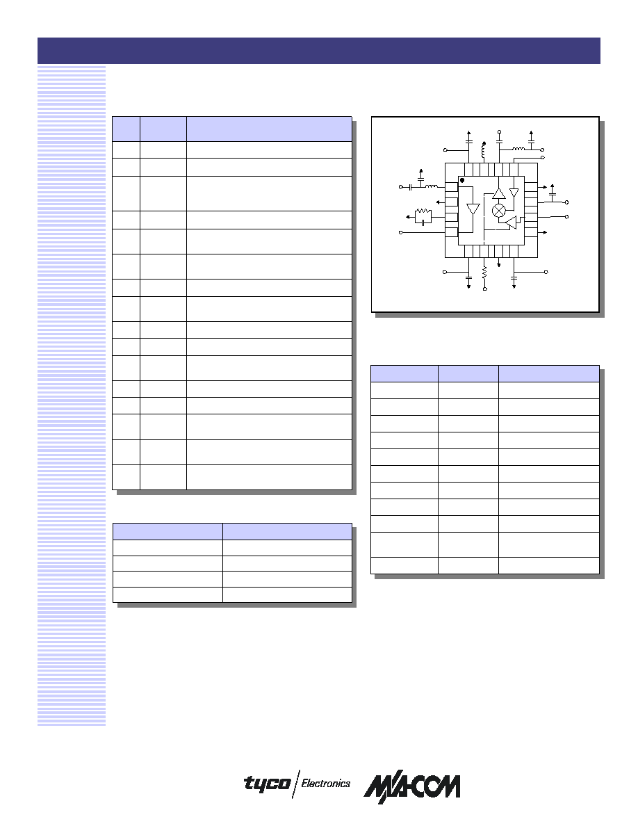
Sample Board Schematic
2. Exceeding any one or combination of these limits may cause
permanent damage to this device
.
L1
LOA VDD
C1
LNA IN
LNA OUT
LOA IN
C4
L2
RFA VDD
IFA OUT
C6
R1
C5
C2
C3
VCTL
R2
LNA VDD2
RFA IN
IFA VDD
C7
C8
L3
C9
LNA VDD1
1
16
1
16
L1
LOA VDD
C1
LNA IN
LNA OUT
LOA IN
C4
L2
RFA VDD
IFA OUT
C6
R1
C5
C2
C3
VCTL
R2
LNA VDD2
RFA IN
IFA VDD
C7
C8
L3
C9
LNA VDD1
1
16
1
16
Part
Value
Purpose
C1
10 pF
LNA Input Matching
C2
1.2 pF
LNA Input Matching
C3
0.1 µF
LNA Source Bypass
C4, C5, C6, C9
0.1 µF
RF Bypass
C7
0.1 µF
IF Bypass
C8
6.8 pF
IF Matching
L1
6.2 nH
LNA Matching
L2
47 nH
IF Output Matching
L3
120 nH
IF Mixer Matching
R1
Optional Resistor to
increase LNA IIP3
R2
3000 Ohms
Voltage Control Resistor
External Circuitry Parts List
(Korean Band PCS)
Parameter
Absolute Maximum
Voltage
6 V
Input Power
0 dBm
Operating Temperature
-30∞C to +85∞C
Storage Temperature
-65∞C to +150∞C

PCS LNA/Downconverter, 1800 - 2000 MHz
MADCSM0012
V 1.00
M/A-COM Inc. and its affiliates reserve the right to make changes to the product(s)
or information contained herein without notice.
Visit www.macom.com for additional data sheets and product information.
n
North America: Tel. (800) 366-2266
n
Asia/Pacific: Tel.+81-44-844-8296, Fax +81-44-844-8298
n
Europe: Tel. +44 (1344) 869 595, Fax+44 (1344) 300 020
3
Recommended PCB Configuration
Operating Instructions
M/A-COM's MADCSM0012 is a highly integrated
MMIC LNA/downconverter for operation in the 1800-
2000 MHz PCS frequency band. The downconverter
provides exceptional RF performance while consuming
low DC current and is packaged in a low cost plastic
package. It is ideal for lightweight battery operated
portable radio systems.
The MADCSM0012 consists of an LNA, RFA, single-
ended mixer and single-ended IF output buffer as shown
in the block diagram. Surface mount resistors, inductors
and capacitors are used in conjunction with the LNA/
downconverter to optimize the trade-offs among
performance, tunability and ease of use. The sample
board schematic shows the LNA/downconverter and
required off-chip components.
The input of the LNA is matched externally with a series
inductor (L1) and a shunt capacitor (C1) to provide a low
loss match to the optimum noise impedance in the band of
interest. A high Q inductor such as Coilcraft's 0402CS
series must be used if the specified noise figures are to be
achieved. The series capacitor, C2, is a DC blocking and
input matching capacitor. The LNA is nominally biased
with 15 mA to give an input IP3 of +6 dBm. An external
resistor, R1, may be used to increase the LNA bias current
and thus increase the IP3. An external image reject filter
is required between the LNA output and RFA input to
prevent downconversion of noise at the image frequency
to the IF. This filter should have a 50-ohm input and
output impedance.
The mixer is a single-ended floating FET mixer that
provides exceptional linearity and isolation with low loss
and no DC current. An off-chip inductor, L3, is required
to match the output of the mixer to the input of the IF
buffer amplifier. The case size of L3 is typically 0603 but
if more gain is needed, use a 0805 case size.
The IF output port is the open drain of the IF buffer
amplifier. This allows maximum flexibility of the
intermediate frequency and also IF filter. A matching
network such as that shown herein can be used to match to
50 ohms from the output impedance of the buffer to the
input impedance of the filter at the 210 MHz
intermediate frequency. The inductor also acts as a choke
for the DC supply line. Elements L2 and C8 provide the
necessary impedance transformation.
The LO input port is matched on-chip to 50 ohms. An
LO buffer amplifier amplifies the -10 dBm input signal
to the level required to drive the mixer. Performance is
optimum with a drive level of -7 dBm.
All DC supply lines must be properly bypassed at RF
frequencies to obtain optimum performance and at
lower frequency to maintain unconditional stability.
Capacitors C4, C5, C6, C7 and C9 are RF bypass
capacitors for the LNA, RFA and LOA. The value and
placement of these capacitors is critical in determining
the frequency response of these amplifiers. Capacitor
C3 is a source bypass capacitor for the second stage of
the low noise amplifier. The placement of this
capacitor will affect the gain of the LNA. For best
performance, all the RF bypass capacitors should be
placed as close to the device as possible.

PCS LNA/Downconverter, 1800 - 2000 MHz
MADCSM0012
V 1.00
M/A-COM Inc. and its affiliates reserve the right to make changes to the product(s)
or information contained herein without notice.
Visit www.macom.com for additional data sheets and product information.
n
North America: Tel. (800) 366-2266
n
Asia/Pacific: Tel.+81-44-844-8296, Fax +81-44-844-8298
n
Europe: Tel. +44 (1344) 869 595, Fax+44 (1344) 300 020
4
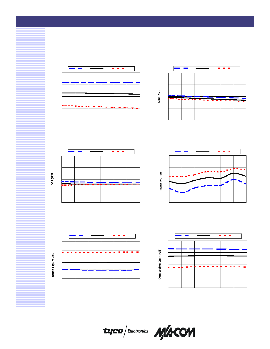
Typical Performance Curves vs. Temperature
LNA Output Return Loss
LNA Gain
LNA Input Return Loss
LNA Input IP3
LNA Noise Figure
13
14
15
16
17
1840
1845
1850
1855
1860
1865
1870
Frequency (MHz)
Gain
(d
B)
-30∞C
+25∞C
+85∞C
-20
-15
-10
-5
0
1840
1845
1850
1855
1860
1865
1870
Frequency (MHz)
-30∞C
+25∞C
+85∞C
-20
-15
-10
-5
0
1840
1845
1850
1855
1860
1865
1870
Frequency (MHz)
-30∞C
+25∞C
+85∞C
2
4
6
8
10
1840
1845
1850
1855
1860
1865
1870
Frequency (MHz)
-30∞C
+25∞C
+85∞C
0.0
0.5
1.0
1.5
2.0
2.5
1840
1845
1850
1855
1860
1865
1870
Frequency (MHz)
-30∞C
+25∞C
+85∞C
Full Chain Conversion Gain
20
22
24
26
28
1840
1845
1850
1855
1860
1865
1870
Frequency (MHz)
-30∞C
+25∞C
+85∞C

PCS LNA/Downconverter, 1800 - 2000 MHz
MADCSM0012
V 1.00
M/A-COM Inc. and its affiliates reserve the right to make changes to the product(s)
or information contained herein without notice.
Visit www.macom.com for additional data sheets and product information.
n
North America: Tel. (800) 366-2266
n
Asia/Pacific: Tel.+81-44-844-8296, Fax +81-44-844-8298
n
Europe: Tel. +44 (1344) 869 595, Fax+44 (1344) 300 020
5
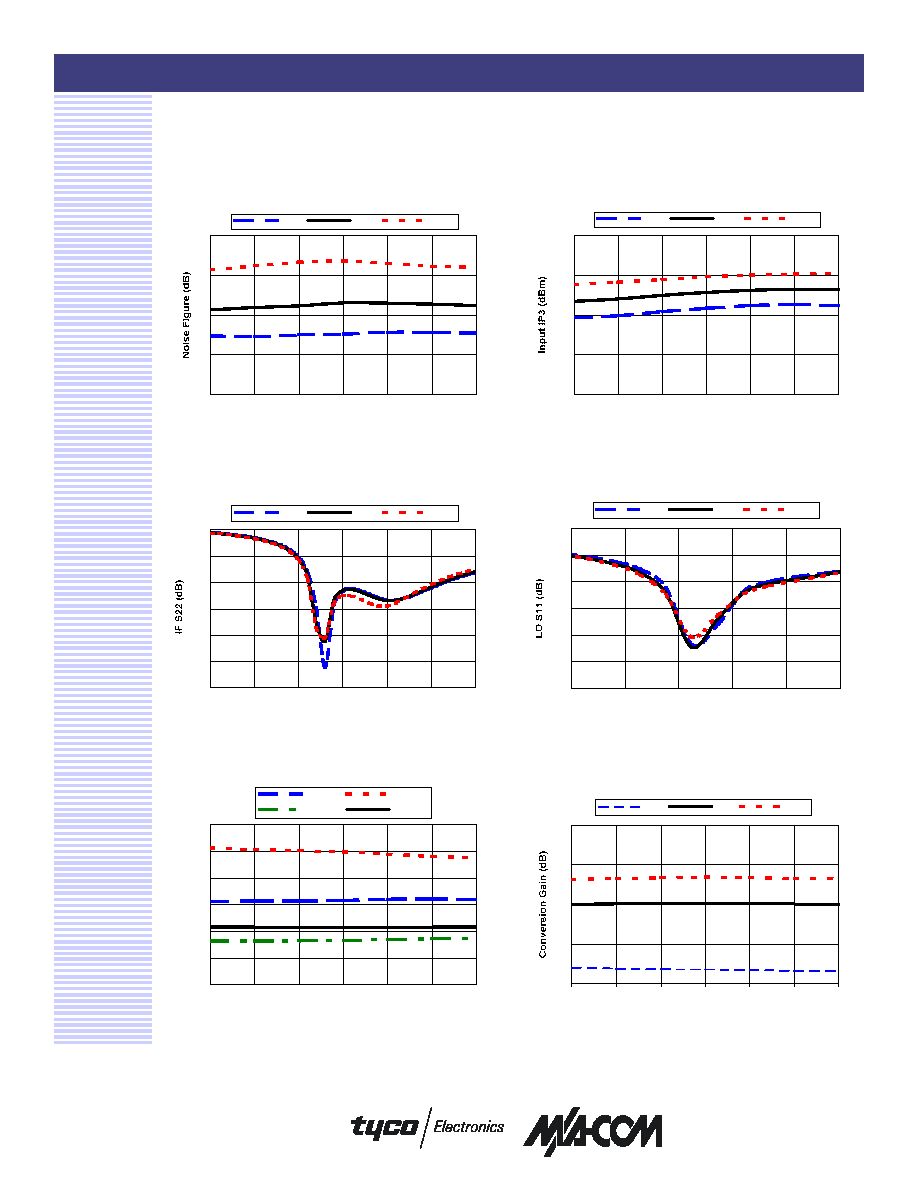
Typical Performance Curves vs. Temperature
Full Chain Noise Figure
Full Chain Input IP3
Full Chain IF Return Loss
Full Chain LO Return Loss
Full Chain Port to Port Isolation
0
1
2
3
4
1840
1845
1850
1855
1860
1865
1870
Frequency (MHz)
-30∞C
+25∞C
+85∞C
-14
-12
-10
-8
-6
1840
1845
1850
1855
1860
1865
1870
Frequency (MHz)
-30∞C
+25∞C
+85∞C
-30
-25
-20
-15
-10
-5
0
150
175
200
225
250
275
300
Frequency (MHz)
-30∞C
+25∞C
+85∞C
-30
-25
-20
-15
-10
-5
0
1200
1400
1600
1800
2000
2200
Frequency (MHz)
-30∞C
+25∞C
+85∞C
0
10
20
30
40
50
60
1840
1845
1850
1855
1860
1865
1870
Frequency (MHz)
I
s
ol
ati
on (dB
)
LO-to-IF
LO-to-RF
RF-to-IF
RF-to-LO
Full Chain Conversion Gain vs. V
CTL
20
22
24
26
28
1840
1845
1850
1855
1860
1865
1870
Frequency MHz)
1.0 V
2.0 V
3.0 V

PCS LNA/Downconverter, 1800 - 2000 MHz
MADCSM0012
V 1.00
M/A-COM Inc. and its affiliates reserve the right to make changes to the product(s)
or information contained herein without notice.
Visit www.macom.com for additional data sheets and product information.
n
North America: Tel. (800) 366-2266
n
Asia/Pacific: Tel.+81-44-844-8296, Fax +81-44-844-8298
n
Europe: Tel. +44 (1344) 869 595, Fax+44 (1344) 300 020
6
Ordering Information
Part Number
Package
MADCSM0012
Bulk Packaging
MADCSM0012TR
Tape and Reel (1K Reel)
MADCSM0012SMB
Sample Test Board
FQFP-N, 3mm, 16 Lead
Note: Reference Application Note M513 for reel size
information.
