Surface Mount Monolithic Integrated PIN Diode Chip:
0604 Unconnected Double Tee
M/A-COM Inc. and its affiliates reserve the right to make changes to the
product(s) or information contained herein without notice. M/A-COM makes
no warranty, representation or guarantee regarding the suitability of its
products for any particular purpose, nor does M/A-COM assume any liability
whatsoever arising out of the use or application of any product(s) or
information.
∑ North America Tel: 800.366.2266 / Fax: 978.366.2266
∑ Europe Tel: 44.1908.574.200 / Fax: 44.1908.574.300
∑ Asia/Pacific Tel: 81.44.844.8296 / Fax: 81.44.844.8298
Visit www.macom.com for additional data sheets and product information.
1
MADP-064908-131000
Surmount
TM
PIN Chip V1
Features
∑
No Wirebonds Required
∑
Rugged Silicon-Glass Construction
∑
Silicon Nitride Passivation & Polymer Scratch
Protection
∑
Ultra-Low Parasitic Capacitance and Inductance
∑
Higher RF C.W. Power Handling
∑
Better Performance than Alternative Packaged
Devices
Description and Applications
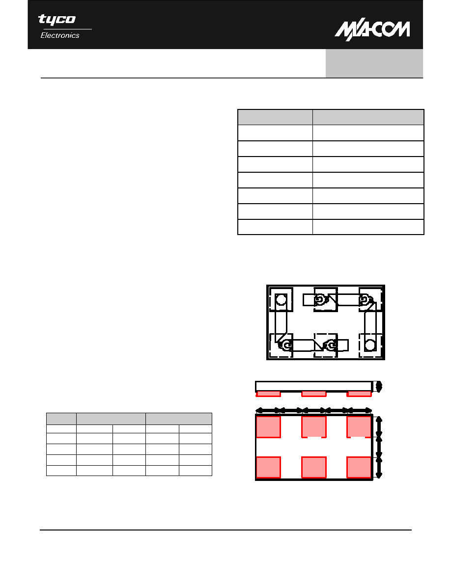
This device is a Silicon-Glass PIN diode chip fabricated with
M/A-COM's patented HMIC process. This 8.0
µ
m
I-region length device features 6 silicon pedestals
embedded in a low loss, low dispersion glass. The
diodes are formed on the top of a pedestal and
connections to the backside of the device are
facilitated by making the pedestal sidewalls
electrically conductive. Selective backside metallization is
applied producing a surface mount device. The
topside is fully encapsulated with silicon nitride and
has an additional polymer layer for scratch
protection. These protective coatings prevent
damage to the junction and the anode air-bridge
during handling and assembly. The vertical Silicon
Diode topology provides for a highly efficient heat
transfer medium.
These packageless devices are suitable for usage in
Higher ( 3 W Avg ) Incident Power Switches. Small
Parasitic Inductance and Excellent RC Constant
make the devices ideal for Absorptive SPST,
Reflective SP2T Switches, and Attenuator Circuits,
where higher P1db and Power Handling values are
required.
Absolute Maximum Ratings
1
@ T
A
= +25 ∞C
(unless otherwise specified)
1. Operation of this device above any one of these parameters
may cause permanent damage.
Parameter
Absolute Maximum
Forward Current
250 mA
Reverse Voltage
l ≠100 V l
Operating Temperature
-55 ∞C to +125 ∞C
Storage Temperature
-55 ∞C to +150 ∞C
Junction Temperature
+175 ∞C
C.W. Incident Power (dBm)
Mounting Temperature
+300 ∞C for 10 seconds
+35 dBm
Dim
Inches
Millimeters
Min.
Max.
Min.
Max.
A
0.060
0.062
1.524
1.575
B
0.036
0.038
0.914
0.965
C
0.004
0.008
0.102
0.203
D
0.011
0.012
0.279
0.305
0604 Case Style - ODS-1310 (Topview)
1. Backside Metal: 0.1microns thick.
2. Shaded Areas Indicate Backside Ohmic Gold Contacts.
C
D D D D D
D
D
D
Side View
4
3
2
1
6
5
Circuit Side
1
2
6
3
5
4

Surface Mount Monolithic Integrated PIN Diode Chip:
0604 Unconnected Double Tee
M/A-COM Inc. and its affiliates reserve the right to make changes to the
product(s) or information contained herein without notice. M/A-COM makes
no warranty, representation or guarantee regarding the suitability of its
products for any particular purpose, nor does M/A-COM assume any liability
whatsoever arising out of the use or application of any product(s) or
information.
∑ North America Tel: 800.366.2266 / Fax: 978.366.2266
∑ Europe Tel: 44.1908.574.200 / Fax: 44.1908.574.300
∑ Asia/Pacific Tel: 81.44.844.8296 / Fax: 81.44.844.8298
Visit www.macom.com for additional data sheets and product information.
2
MADP-064908-131000
Surmount
TM
PIN Chip V1
Electrical Specifications @ +25 ∞C, per Diode Junction
Symbol
Conditions
Units
Min.
Typ.
Max.
C
T
-40 V, 1 MHz
1
pF
0.05
0.07
C
T
-40 V, 1 GHz
1,3
pF
0.04
0.06
R
S
10 mA, 1 GHz
2,3
5.0
V
F
10 mA
V
0.83
1.00
V
R
-10
µ
A
V
l ≠70 l
l ≠100 l
I
R
-70 V
µ
A
l ≠0.1 l
l ≠10 l
T
L
+ 10 mA / -6 mA
ns
200
TH
1A / 10 mA
∞
C / W
150
1. Total capacitance, C
T
, is equivalent to the sum of Junction Capacitance ,Cj, and Parasitic Capacitance, Cpar.
2. Series resistance R
S
is equivalent to the total diode resistance : Rs = Rj ( Junction Resistance) + Rc ( Ohmic Resistance)
3. Rs, C
T,
T
L,
TH
are measured on an HP4291A Impedance Analyzer with die mounted in an ODS-186 package with Sn 60/Pb 40 Solder
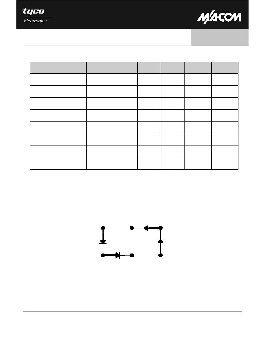
Equivalent 0604 Style Double Tee Equivalent Circuit
1
2
3
5
6
4
Top View
Notes:
1. Ports 2 and 5 have a Connected Cathode-Anode Node.
2. Ports 1,3,4, and 6 Have a Singular, Un-Connected Node.

Surface Mount Monolithic Integrated PIN Diode Chip:
0604 Unconnected Double Tee
M/A-COM Inc. and its affiliates reserve the right to make changes to the
product(s) or information contained herein without notice. M/A-COM makes
no warranty, representation or guarantee regarding the suitability of its
products for any particular purpose, nor does M/A-COM assume any liability
whatsoever arising out of the use or application of any product(s) or
information.
∑ North America Tel: 800.366.2266 / Fax: 978.366.2266
∑ Europe Tel: 44.1908.574.200 / Fax: 44.1908.574.300
∑ Asia/Pacific Tel: 81.44.844.8296 / Fax: 81.44.844.8298
Visit www.macom.com for additional data sheets and product information.
3
MADP-064908-131000
Surmount
TM
PIN Chip V1
Assembly Guidelines
Handling
All semiconductor chips should be handled with care to avoid damage or contamination from perspiration and
skin oils. The use of plastic tipped tweezers or vacuum pickups is strongly recommended for individual
components. Bulk handling should insure that abrasion and mechanical shock are minimized.
Bonding
Attachment to a circuit board is made simple through the use of surface mount technology. Mounting pads are
conveniently located on the bottom surface of these devices and are removed from the active junction locations.
These devices are well suited for solder attachment onto hard and soft substrates. The use of
80 Au / 20 Sn or Sn 60 / Pb 40 solder is recommended. Conductive silver epoxy for die attachment, approximately
2 mils in uniform thickness may also be used for lower Incident power applications ( < 1 W Average Power ).
When soldering these devices to a hard substrate, hot gas die bonding is preferred. We recommend utilizing a
vacuum tip and force of 60 to 100 grams applied normal to the top surface of the device. When soldering to soft
substrates, it is recommended to use a lead-tin interface at the circuit board mounting pads. Position the die so
that its mounting pads are aligned with the circuit board mounting pads and reflow the solder by heating the
circuit trace near the mounting pad while applying 60 to 100 grams of force perpendicular to the top surface of
the die. The solder joint must Not be made one at a time, creating un-equal heat flow and thermal stress. Solder
reflow should Not be performed by causing heat to flow through the top surface of the die. Since the HMIC glass
is transparent, the edges of the mounting pads closest to each other can be visually inspected through the die
after attach is completed.
A typical profile for a Sn 60/ Pb 40 Soldering process is provided in Application Note, " M538 " ,
" Surface Mounting Instructions " on the MA-COM website www.macom.com

Surface Mount Monolithic Integrated PIN Diode Chip:
0604 Unconnected Double Tee
M/A-COM Inc. and its affiliates reserve the right to make changes to the
product(s) or information contained herein without notice. M/A-COM makes
no warranty, representation or guarantee regarding the suitability of its
products for any particular purpose, nor does M/A-COM assume any liability
whatsoever arising out of the use or application of any product(s) or
information.
∑ North America Tel: 800.366.2266 / Fax: 978.366.2266
∑ Europe Tel: 44.1908.574.200 / Fax: 44.1908.574.300
∑ Asia/Pacific Tel: 81.44.844.8296 / Fax: 81.44.844.8298
Visit www.macom.com for additional data sheets and product information.
4
MADP-064908-131000
Surmount
TM
PIN Chip V1
HMIC Die
SN7406, SN7416 TTL Open Collector Gate Driver ( X2 )
J3
J2
B3 Bias
B2 Bias
22 pF
22 pF
22 pF
15 nH
15 nH
+5V
+
5 V
22 pF
+5V
+5V
15 nH
?
?
?
?
1
2
3,6
4
5
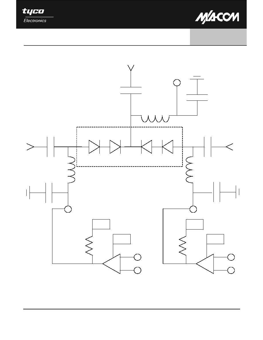
Circuit Applications : SP2T All Series Reflective Switch with +5V and TTL Logic Control
( 2- 18 GHz )
100
100
J1
J22 pF
+1.8 V
22 pF

Surface Mount Monolithic Integrated PIN Diode Chip:
0604 Unconnected Double Tee
M/A-COM Inc. and its affiliates reserve the right to make changes to the
product(s) or information contained herein without notice. M/A-COM makes
no warranty, representation or guarantee regarding the suitability of its
products for any particular purpose, nor does M/A-COM assume any liability
whatsoever arising out of the use or application of any product(s) or
information.
∑ North America Tel: 800.366.2266 / Fax: 978.366.2266
∑ Europe Tel: 44.1908.574.200 / Fax: 44.1908.574.300
∑ Asia/Pacific Tel: 81.44.844.8296 / Fax: 81.44.844.8298
Visit www.macom.com for additional data sheets and product information.
5
MADP-064908-131000
Surmount
TM
PIN Chip V1
RF Truth Table for Reflective SP2T using Singular Power Supply: + 5V, + I Only
RF State
B2 Diode Bias
B3 Diode Bias
J1 ≠ J2 Low Loss &
J1≠ J3 Isolation
+ 3.6 V @ + 14 mA
+0.5 V @ 0 mA
J1 ≠ J3 Low Loss &
J1≠J2 Isolation
+0.5 V @ 0 mA
+ 3.6 V @ + 14 mA
Notes:
1. Diode Forward Voltage Differential (
Vf ) @ 15 mA = 0.9 V
2. Insertion Loss Diode Bias = ( + 5V ≠ (2)* 0.9 V ≠ 1.8 V ) / ( 100
) = 14 mA
3. Off Isolation Diode Back Bias Voltage = | ≠ ( +1.8 V ≠ 0.5 V ) | = | ≠ 1.3 V |.
