Avionics Pulsed Power Transistor, 700 Watts,
1.03-1.09 GHz, 32 µS Pulse, 2% Duty
Features
Designed for Mode-S IFF Applications
NPN Silicon Microwave Power Transistor
Common Base Configuration
Broadband Class C Operation
High Efficiency Interdigitated Geometry
Gold Metalization System
Internal Input and Output Impedance Matching
Hermetic Metal/Ceramic Package
PH1090-700B
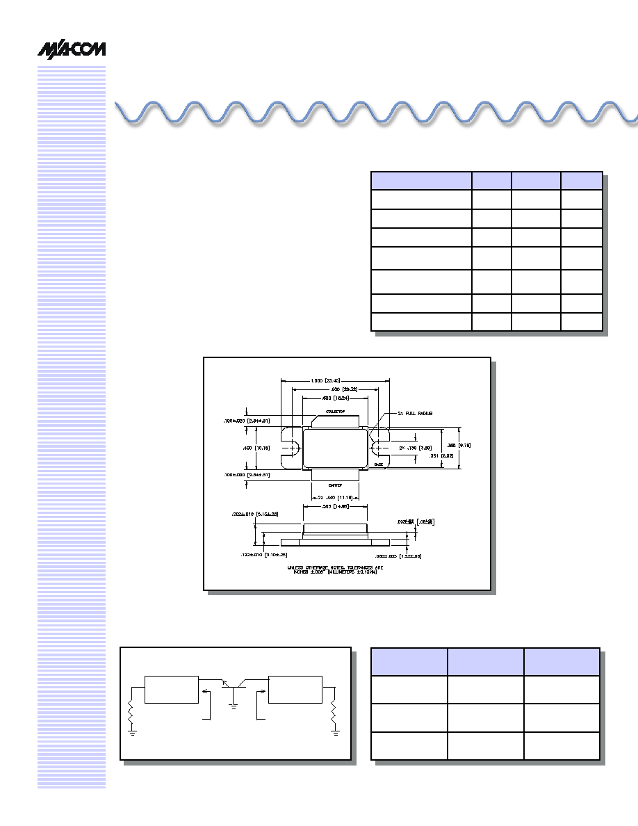
Outline Drawing
12/10/01
Rev. 0
Absolute Maximum Ratings @ 25 ∞C
Parameter
Symbol
Rating
Units
Collector-Emitter Voltage
V
CES
65
V
Emitter-Base Voltage
V
EBO
3.0
V
Collector Current (Peak)
I
C
35
A
Dissipated Power
(Standard Pulse Cond.)
P
TOT
2.9
kW
Dissipated Power
(Mode-S Pulse Train)
P
TOT
700
W
Storage Temperature
T
STG
-65 to +200
∞C
Junction Temperature
T
j
200
∞C
F (GHz)
Z
IF
()
Z
OF
()
1.03
1.1 ≠j1.4
1.2 ≠j0.8
1.06
1.1 ≠j1.2
1.0 ≠j0.7
1.09
1.0 ≠j1.0
0.8 ≠j0.7
Broadband Test Fixture Impedances
TEST FIXTURE
INPUT
CIRCUIT
ZIF
TEST FIXTURE
OUTPUT
CIRCUIT
ZOF
50
50

Avionics Pulsed Power Transistor, 700 Watts, 1.03-1.09 GHz, 32
µS Pulse, 2% Duty
PH1090-700B
12/10/01
Rev. 0
2
Standard Pulse Condition: 32µS Pulse Width, 2% Duty Cycle
Peak Power: 700 Watts
Parameter
Symbol
Test Conditions
Min
Max
Units
Collector-Emitter Breakdown Voltage
BVCES
IC = 250 mA
80
-
V
Collector-Emitter Leakage Current
ICES
VCE = 50 V
-
25
mA
Thermal Resistance
RTH(JC)
V
CC
=50 V, Pout=700 W, F=1.03, 1.09 GHz
Pulse Conditions: 32
µs, 2%
-
0.06
∞C/W
Power Gain
GP
V
CC
=50 V, Pout=700 W, F=1.03, 1.09 GHz
Pulse Conditions: 32
µs, 2%
7.5
-
dB
Collector Efficiency
V
CC
=50 V, Pout=700 W, F=1.03, 1.09 GHz
Pulse Conditions: 32
µs, 2%
50
-
%
Input Return Loss
RL
V
CC
=50 V, Pout=700 W, F=1.03, 1.09 GHz
Pulse Conditions: 32
µs, 2%
-10
-
dB
Load Mismatch Tolerance
VSWR-T
V
CC
=50 V, Pout=700 W, F=1.03, 1.09 GHz
Pulse Conditions: 32
µs, 2%
-
5.0:1
-
Load Mismatch Stability
VSWR-S
V
CC
=50 V, Pout=700 W, F=1.03, 1.09 GHz
Pulse Conditions: 32
µs, 2%
-
1.5:1
-
Electrical Characteristics at 25∫C
Parameter
Symbol
Test Conditions
Typical
Units
Thermal Resistance
RTH(JC)
V
CC
=45v, Pout=450 W, F=1.03, 1.09 GHz
Mode-S Pulse Train
0.20
∞C/W
Power Gain
GP
V
CC
=45v, Pout=450 W, F=1.03, 1.09 GHz
Mode-S Pulse Train
8.0
dB
Collector Efficiency
V
CC
=45v, Pout=450 W, F=1.03, 1.09 GHz
Mode-S Pulse Train
55
%
Input Return Loss
RL
V
CC
=45v, Pout=450 W, F=1.03, 1.09 GHz
Mode-S Pulse Train
-13
dB
Load Mismatch Tolerance
VSWR-T
V
CC
=45v, Pout=450 W, F=1.03, 1.09 GHz
Mode-S Pulse Train
2:1
-
Load Mismatch Stability
VSWR-S
V
CC
=45v, Pout=450 W, F=1.03, 1.09 GHz
Mode-S Pulse Train
1.5:1
-
Mode-S Pulse Train: 48 Pulses of 32µS "on", 18µS "off" repeated
every 24 mS, 6.4% Overall Duty Cycle**
Peak Power: 450 Watts
** Please note, the standard PH1090-700B device will be tested in accordance with the specifications defined for
the Standard Pulse Condition (32µS, 2%)

Avionics Pulsed Power Transistor, 700 Watts, 1.03-1.09 GHz, 32
µS Pulse, 2% Duty
PH1090-700B
12/10/01
Rev. 0
Specifications subject to change without notice.
North America: Tel. (800) 366-2266
Asia/Pacific: Tel.+81-44-844-8296, Fax +81-44-844-8298
Europe: Tel. +44 (1344) 869 595, Fax+44 (1344) 300 020
Visit www.macom.com for additional data sheets and product information.
4
Broadband Assembly Diagram
Broadband Circuit Dimensions


