 | –≠–ª–µ–∫—Ç—Ä–æ–Ω–Ω—ã–π –∫–æ–º–ø–æ–Ω–µ–Ω—Ç: SMLW010A | –°–∫–∞—á–∞—Ç—å:  PDF PDF  ZIP ZIP |

Data Sheet
January 2002
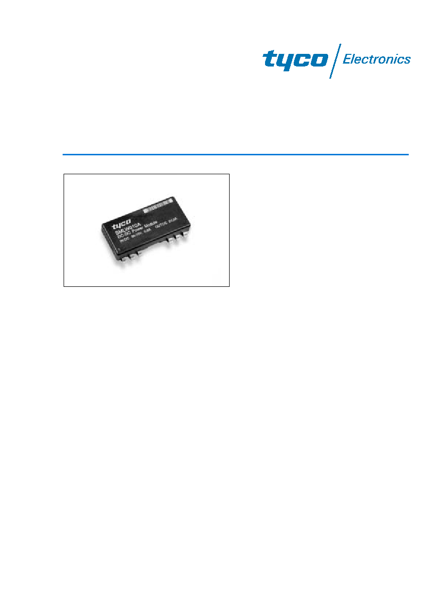
SMLW010 Single-Output Low-Profile
Power Modules: 36 Vdc to 75 Vdc Input; 10 W
The SMLW010 Single-Output, Low-Profile, PCB Mount Power
Modules use advanced, surface-mount technology and
deliver high-quality, compact, dc-dc conversion at an eco-
nomical price.
Applications
Communications equipment
Computer equipment
Distributed power architectures
Surface-mount applications
Features
Low profile: 8.2 mm x 22.6 mm x 47.8 mm
(0.323 in. x 0.89 in. x 1.88 in.)
Wide input voltage range: 36 Vdc to 75 Vdc
Input-to-output isolation: 1500 V
Operating case temperature range: ≠40 ∞C to
+105 ∞C
Overcurrent protection, unlimited duration
Positive remote on/off logic
Output voltage adjustment: 90% to 110% of V
O, nom
Output overvoltage protection
Undervoltage lockout
UL* 60950 Recognized, CSA
C22.2 No. 60950-00
Certified, VDE 0805 (EN60950) Licensed
CE mark meets 73/23/EEC and 93/68/EEC
directives
Within FCC Class A radiated limits
Options
Synchronization
Description
The SMLW010 Single-Output, Low-Profile, PCB Mount Power Modules are low-profile, dc-dc converters that
operate over an input voltage range of 36 Vdc to 75 Vdc and provide a precisely regulated output. The output is
isolated from the input, allowing versatile polarity configurations and grounding connections. Built-in filtering for
both input and output minimizes the need for external filtering. These modules are designed and manufactured
to be gull-winged surface-mounted power modules that are reflowed with other surface-mount components in a
typical surface-mount fashion.
*
UL is a registered trademark of Underwriters Laboratories, Inc.
CSA is a registered trademark of Canadian Standards Association.
This product is intended for integration into end-use equipment. All the required procedures for CE marking of end-use equipment should
be followed. (The CE mark is placed on selected products.)

2
Tyco Electronics Corp.
Data Sheet
January 2002
Power Modules: 36 Vdc to 75 Vdc Input; 10 W
SMLW010 Single-Output Low-Profile
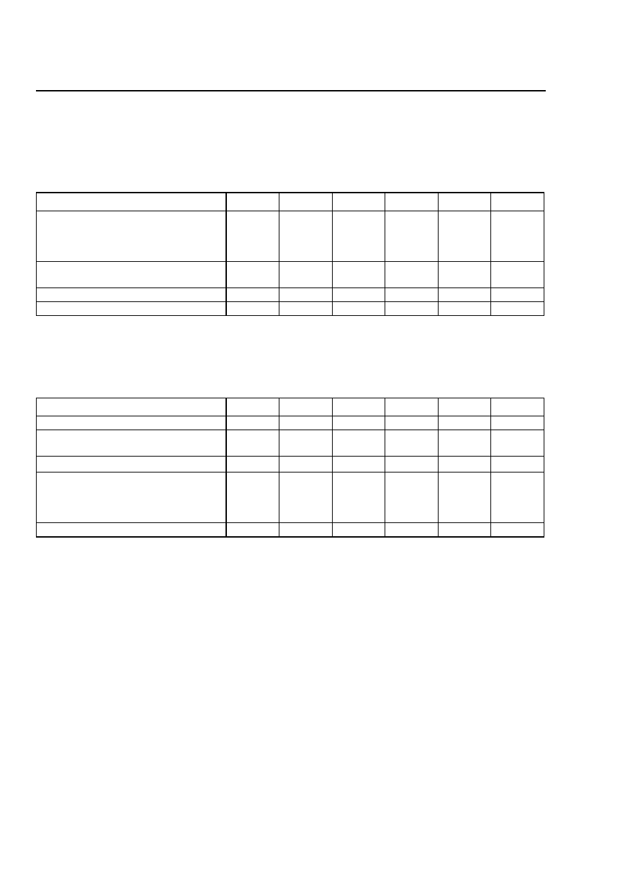
Absolute Maximum Ratings
Stresses in excess of the absolute maximum ratings can cause permanent damage to the device. These are
absolute stress ratings only. Functional operation of the device is not implied at these or any other conditions in
excess of those given in the operations sections of the data sheet. Exposure to absolute maximum ratings for
extended periods can adversely affect device reliability.
* See derating curves, Figure 8, for details.
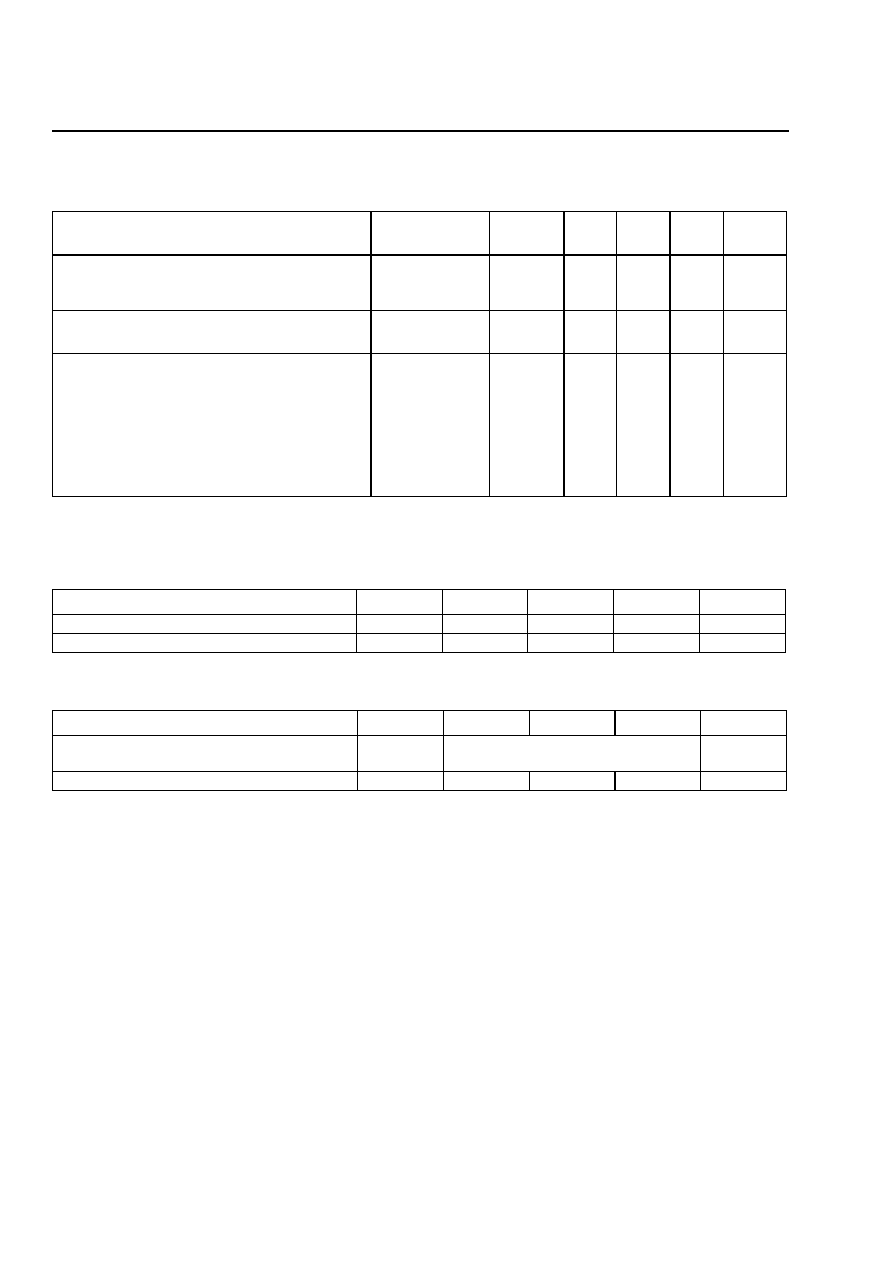
Electrical Specifications
Table 1. Input Specifications
Fusing Considerations
CAUTION: This power module is not internally fused. An input line fuse must always be used.
This encapsulated power module can be used in a wide variety of applications, ranging from simple stand-alone
operation to an integrated part of a sophisticated power architecture. To preserve maximum flexibility, internal
fusing is not included; however, to achieve maximum safety and system protection, always use an input line fuse.
The safety agencies require a normal-blow fuse with a maximum rating of 5 A (see Safety Considerations section).
Based on the information provided in this data sheet on inrush energy and maximum dc input current, the same
type of fuse with a lower rating can be used. Refer to the fuse manufacturer's data for further information.
Parameter
Device
Symbol
Min
Typ
Max
Unit
Input Voltage:
Continuous
Transient (100 ms)
SMLW
All
V
I
V
I, trans
0
0
--
--
80
100
Vdc
V
Operating Case Temperature
(See Thermal Considerations section.)
All
T
C
≠40
--
105*
∞C
Storage Temperature
All
T
stg
≠55
--
125
∞C
I/O Isolation Voltage (for 1 minute)
All
--
--
--
1500
Vdc
Parameter
Device
Symbol
Min
Typ
Max
Unit
Operating Input Voltage
SMLW
V
I
36
48
75
Vdc
Maximum Input Current
(V
I
= 0 to V
I, max
; I
O
= I
O, max
)
SMLW
I
I, max
--
--
0.6
A
Inrush Transient
All
I
2
t
--
--
0.2
A
2
s
Input Reflected-ripple Current
(5 Hz to 2 0MHz; 12 µH source imped-
ance; T
A
= 25 ∞C; see Figure 1 and
Design Considerations section.)
All
I
I
--
2
--
mAp-p
Input Ripple Rejection (100 Hz--120 Hz)
All
--
--
50
--
dB

Tyco Electronics Corp.
3
Data Sheet
January 2002
Power Modules: 36 Vdc to 75 Vdc Input; 10 W
SMLW010 Single-Output Low-Profile
Electrical Specifications
(continued)
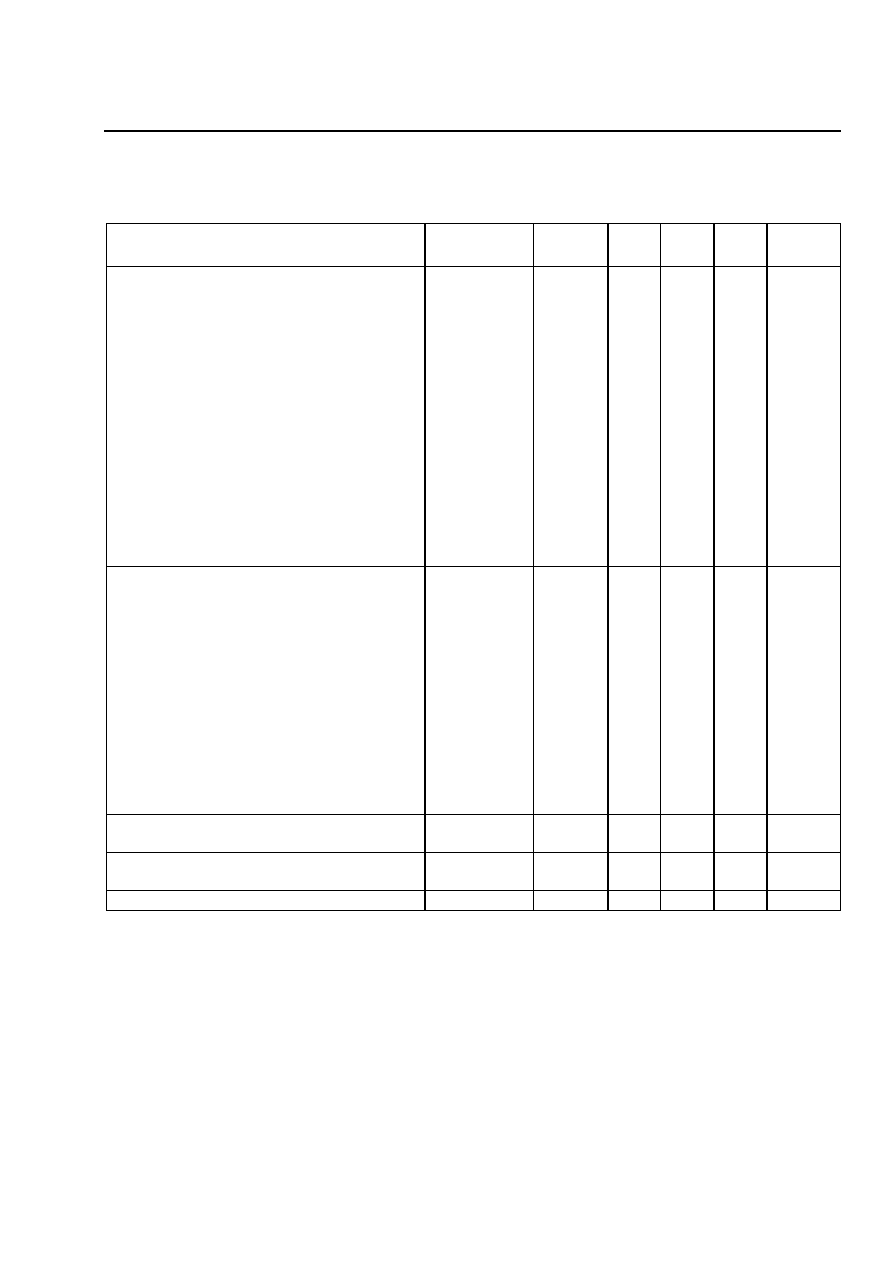
Table 2. Output Specifications
* For output voltages below 2.5 V, the G is trimmable down to 1.5 V.
Parameter
Device Code
or Suffix
Symbol
Min
Typ
Max
Unit
Output Voltage Set Point
(V
I
= V
I, nom
; I
O
= I
O, max
; T
A
= 25 ∞C)
G*
A
V
O, set
V
O, set
2.45
4.85
2.5
5.0
2.55
5.15
Vdc
Vdc
Output Voltage
(Over all line, load, and temperature conditions
until end of life; see Figure 3.)
G
A
V
O
V
O
2.41
4.80
--
--
2.59
5.20
Vdc
Vdc
Output Regulation:
Line (V
I
= V
I, min
to V
I, max
)
Load (I
O
= I
O, min
to I
O, max
)
Temperature (T
C
= ≠40 ∞C to +85 ∞C)
A, G
A, G
A, G
--
--
--
--
--
--
--
--
--
--
--
--
1
0.01
10
0.1
25
0.5
--
--
--
--
--
--
mV
%V
O
mV
%V
O
mV
%V
O
Output Ripple and Noise Voltage
(Across one 0.1 µF ceramic capacitor; see
Figure 2.):
RMS
Peak-to-peak (5 Hz to 20 MHz)
A, G
A, G
--
--
--
--
--
--
25
75
mVrms
mVp-p
External Load Capacitance
A, G
--
0
--
220
µF
Output Current
(At I
O
< I
O, min
, the modules may exceed output
ripple specifications, but operation is guaran-
teed. For A, and G codes, the output voltage
may exceed specifications when I
O
< I
O, min
.)
G
A
I
O
I
O
0.15
0.10
--
--
3.0
2.0
A
A
Output Current-limit Inception
(V
O
= 90% V
O, set
)
All
I
O
--
115
--
%I
O, max
Output Short-circuit Current
(V
O
= 0.25 V at 25 ∞C)
All
I
O
--
200
--
%I
O, max

4
Tyco Electronics Corp.
Data Sheet
January 2002
Power Modules: 36 Vdc to 75 Vdc Input; 10 W
SMLW010 Single-Output Low-Profile
Electrical Specifications
(continued)
Table 2. Output Specifications (continued)
* For output voltages below 2.5 V, the G is trimmable down to 1.5 V.
Engineering estimate.
Table 3. Isolation Specifications
Table 4. General Specifications
Parameter
Device Code
or Suffix
Symbol
Min
Typ
Max
Unit
Efficiency
(V
I
= V
I, nom
; I
O
= I
O, max
; T
A
= 25 ∞C; see
Figure 3.)
SMLW010G
SMLW010A
--
--
73
79
--
--
%
%
Switching Frequency
A
G
--
--
--
--
475
350
--
--
kHz
kHz
Dynamic Response
(
I
O
/
t = 1A/10 µs; V
I
= V
I, nom
; T
A
= 25 ∞C):
Load Change from I
O
= 50% to 75% of I
O, max
:
Peak Deviation
Settling Time (V
O
< 10% of peak deviation)
Load Change from I
O
= 50% to 25% of I
O, max
:
Peak Deviation
Settling Time (V
O
< 10% of peak deviation)
All
All
All
All
--
--
--
--
--
--
--
--
3
1.5
3
1.5
--
--
--
--
%V
O, set
ms
%V
O, set
ms
Parameter
Device
Min
Typ
Max
Unit
Isolation Capacitance (engineering estimate)
All
--
1100
--
pF
Isolation Resistance
All
10
--
--
M
Parameter
Device
Min
Typ
Max
Unit
Calculated MTBF
(I
O
= 80% of I
O, max
; T
C
= 40 ∞C)
All
5,500,000
hours
Weight (engineering estimate)
All
--
--
17 (0.6)
g (oz.)

Tyco Electronics Corp.
5
Data Sheet
January 2002
Power Modules: 36 Vdc to 75 Vdc Input; 10 W
SMLW010 Single-Output Low-Profile
Electrical Specifications
(continued)
Table 5. Feature Specifications
Parameter
Device Code
or Suffix
Symbol
Min
Typ
Max
Unit
Remote On/Off Signal Interface
(V
I
= V
I, min
to V
I, max
; open collector or
equivalent compatible; signal referenced to
V
I
(≠) terminal. See Figure 4 and Feature
Descriptions.):
Logic Low--Module Off
Logic High--Module On
Module Specifications:
On/Off Current--Logic Low
On/Off Voltage:
Logic Low
Logic High (I
on/off
= 0 mA)
Open Collector Switch Specifications:
Leakage Current During Logic High
(V
on/off
= 6 V)
Output Low Voltage During Logic Low
(I
on/off
= 1 mA)
All
All
All
All
All
I
on/off
V
on/off
V
on/off
I
on/off
V
on/off
--
≠0.7
--
--
--
--
--
--
--
--
1.0
1.2
6
50
1.2
mA
V
V
µA
V
Turn-on Delay and Rise Times
(at 80% of I
O, max
; T
A
= 25 ∞C):
Case 1: On/Off Input Is Set for Logic High and
then Input Power Is Applied (Delay from
Point at Which V
I
= V
I, min
until V
O
= 10% of
V
O, nom
).
Case 2: Input Power Is Applied for at Least
One Second, and then the On/Off Input Is
Set to Logic High (Delay from Point at Which
V
on/off
= 0.9 V until V
O
= 10% of V
O, nom
).
Output Voltage Rise Time (Time for V
O
to
Rise from 10% of V
O, nom
to 90% of V
O, nom
)
Output Voltage Overshoot (at 80% of I
O, max
;
T
A
= 25 ∞C)
All
All
All
All
T
delay
T
delay
T
rise
--
--
--
--
--
15
4
2
--
60
10
10
5
ms
ms
ms
%
Output Voltage Set Point Adjustment Range
A
G
V
trim
V
trim
90
60
--
--
110
110
%V
O, nom
%V
O, nom
Output Overvoltage Protection (clamp)
G
A
V
O, clamp
V
O, clamp
3.0
5.6
--
--
5.7
7.7
V
V
Undervoltage Lockout
All
--
20
27
--
V

Data Sheet
January 2002
Power Modules: 36 Vdc to 75 Vdc Input; 10 W
SMLW010 Single-Output Low-Profile
6
Tyco Electronics Corp.
Test Configurations
8-203
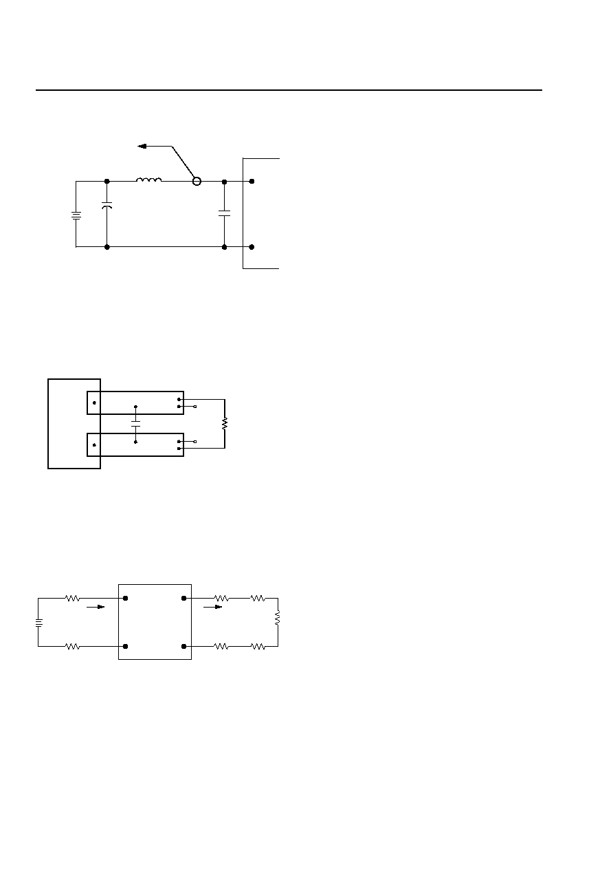
Note: Input reflected-ripple current is measured with a simulated
source impedance of 12 µH. Capacitor Cs offsets possible
battery impedance. Current is measured at the input of the
module.
Figure 1. Input Reflected-Ripple Test Setup
8-513
Note: Use one 0.1 µF ceramic capacitor. Scope measurement should
be made using a BNC socket. Position the load between 50
mm and 75 mm (2 in. and 3 in.) from the module.
Figure 2. Peak-to-Peak Output Noise Measurement
Test Setup
8-204(C)
Note: All measurements are taken at the module terminals. When
socketing, place Kelvin connections at module terminals to
avoid measurement errors due to socket contact resistance.
Figure 3. Output Voltage and Efficiency
Measurement Test Setup
Design Considerations
Input Source Impedance
The power module should be connected to a low
ac-impedance input source. Highly inductive source
impedances can affect the stability of the power mod-
ule. If the source inductance exceeds 10 µH, a 33 µF
electrolytic capacitor (ESR < 0.7
at 100 kHz)
mounted close to the power module helps ensure
stability of the unit. (See Figure 1.)
Solder Recommendations
Large surface-mount components typically require a
thicker stencil than smaller components to ensure a
reliable solder joint. The SMLW010 Single-Output,
Low-Profile, PCB Mount Power Modules have been
evaluated for solder joint reliability and shock and vibra-
tion requirements using 170,000 cubic mils (2. 8mm
3
)
of solder. This volume can be obtained by printing sol-
der 12 mils thick on the copper pads or overprinting the
copper pads 13 mils (0.33 mm) around the pad area
with 8 mils of printed solder. Although this volume is
recommended, tests have been conducted using lower
volumes with successful results. Contact technical sup-
port for further assistance.
TO OSCILLOSCOPE
12 µH
C
S
220 µF
IMPEDANCE < 0.1
@ 20 ∞C, 100 kHz
V
I
(+)
V
I
(-)
BATTERY
33 µF
CURRENT
PROBE
L
TEST
V
O
(+)
V
O
(≠)
RESISTIVE
LOAD
SCOPE
0.1 µF
COPPER STRIP
V
I
(+)
V
I
(-)
V
O
(+)
V
O
(-)
I
I
I
O
SUPPLY
CONTACT RESISTANCE
CONTACT AND
DISTRIBUTION LOSSES
LOAD
V
O
(+)
V
O
(≠)
≠
[
]I
O
V
I
(+)
V
I
(≠)
≠
[
]I
I
-----------------------------------------------
100 %
◊
=

Data Sheet
January 2002
Power Modules: 36 Vdc to 75 Vdc Input; 10 W
SMLW010 Single-Output Low-Profile
Tyco Electronics Corp.
7
Safety Considerations
SMLW Modules
For safety-agency approval of the system in which the
power module is used, the power module must be
installed in compliance with the spacing and separation
requirements of the end-use safety agency standard,
i.e.,
UL 60950, CSA C22.2 No. 60950-00, and VDE
0805 (EN60950).
If the input source is non-SELV (ELV or a hazardous
voltage greater than 60 Vdc and less than or equal to
75 Vdc), for the module's output to be considered
meeting the requirements of safety extra-low voltage
(SELV), all of the following must be true:
The input source is to be provided with reinforced
insulation from any other hazardous voltages, includ-
ing the ac mains.
One V
I
pin and one V
O
pin are to be grounded or
both the input and output pins are to be kept floating.
The input pins of the module are not operator acces-
sible.
Another SELV reliability test is conducted on the
whole system, as required by the safety agencies, on
the combination of supply source and the subject
module to verify that under a single fault, hazardous
voltages do not appear at the module's output.
Note: Do not ground either of the input pins of the
module without grounding one of the output
pins. This may allow a non-SELV voltage to
appear between the output pins and ground.
The power module has extra-low voltage (ELV) outputs
when all inputs are ELV.
The input to these units is to be provided with a maxi-
mum 5 A normal-blow fuse in the ungrounded lead.
Feature Descriptions
Overcurrent Protection
To provide protection in a fault (output overload) condi-
tion, the unit is equipped with internal current-limiting
circuitry and can endure current limiting for an unlim-
ited duration. At the point of current-limit inception, the
unit shifts from voltage control to current control. If the
output voltage is pulled very low during a severe fault,
the current-limit circuit can exhibit either foldback or
tailout characteristics (output-current decrease or
increase). The unit operates normally once the output
current is brought back into its specified range.
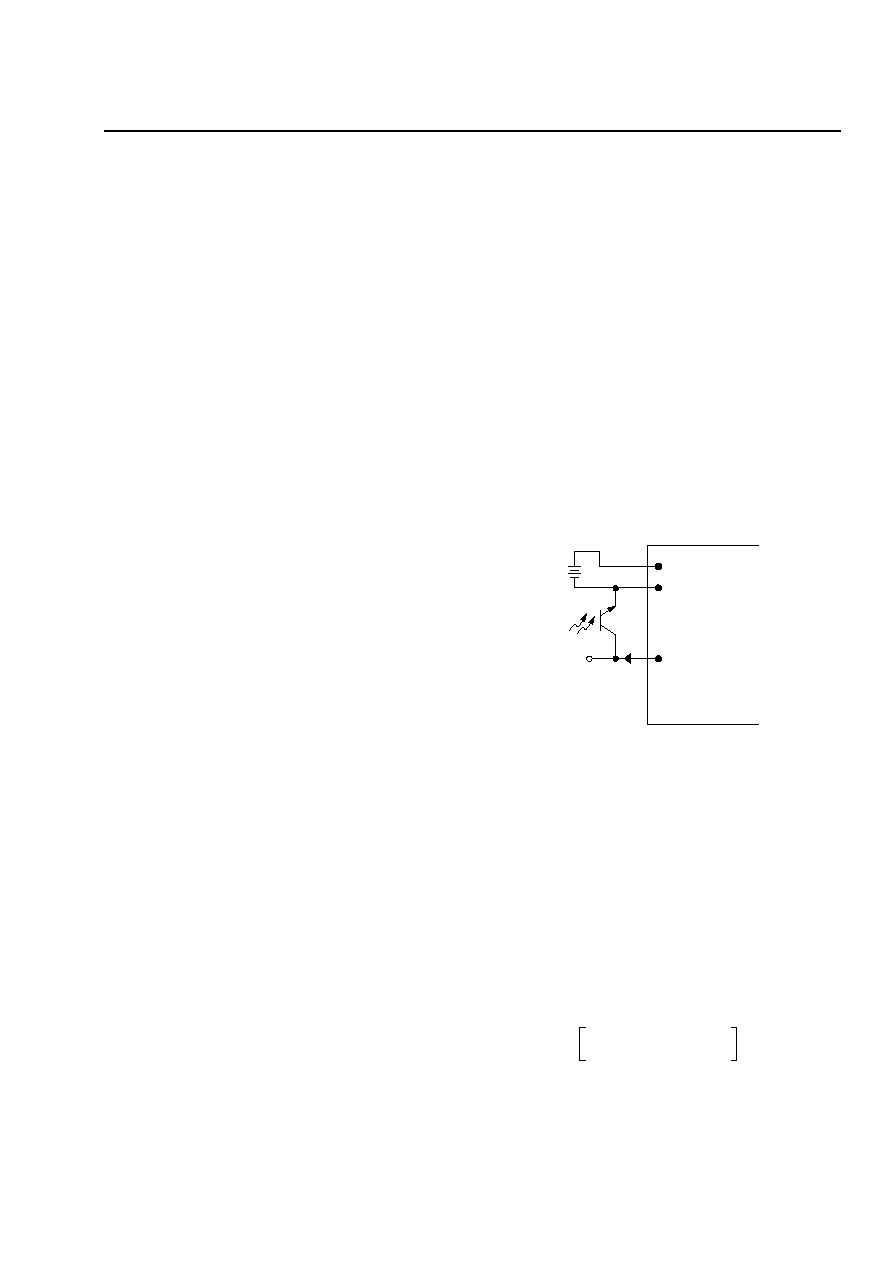
Remote On/Off
Positive logic remote on/off turns the module on during
a logic-high voltage on the remote ON/OFF pin, and off
during a logic low.
To turn the power module on and off, the user must
supply a switch to control the voltage between the
on/off terminal and the V
I
(≠) terminal (V
on/off
). The
switch may be an open collector or equivalent (see
Figure 4). A logic low is V
on/off
= ≠0.7 V to 1.2 V. The
maximum I
on/off
during a logic low is 1 mA. The switch
should maintain a logic-low voltage while sinking 1 mA.
During a logic high, the maximum V
on/off
generated by
the power module is 6 V. The maximum allowable leak-
age current of the switch at V
on/off
= 6 V is 50 µA.
The module has internal capacitance to reduce noise
at the ON/OFF pin. Additional capacitance is not gen-
erally needed and may degrade the start-up character-
istics of the module.
8-758a
Figure 4. Remote On/Off Implementation
Output Voltage Adjustment
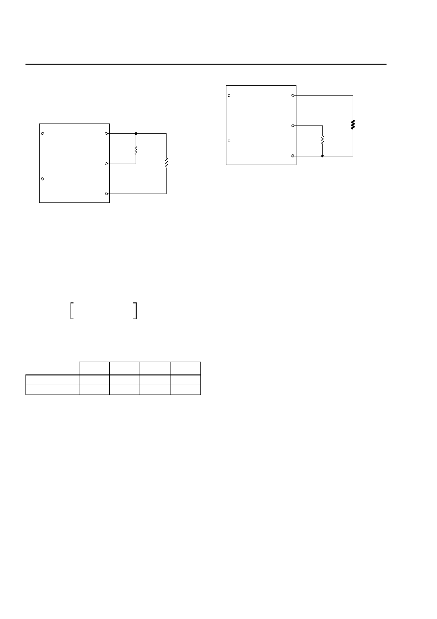
Output voltage set-point adjustment allows the user to
increase or decrease the output voltage set point of a
module. This is accomplished by connecting an exter-
nal resistor between the TRIM pin and either the V
O
(+)
or V
O
(≠) pins. With an external resistor between the
TRIM and V
O
(+) pins (R
adj-down
), the output voltage set
point (V
O, adj
) decreases (see Figure 5). The following
equation determines the required external resistor
value to obtain an output voltage change from V
O, nom
to
V
O, adj
:
where R
adj-down
is the resistance value connected
between TRIM and V
O
(+), and G, H, and L are defined
in the table below.
+
I
on/off
-
V
on/off
REMOTE
ON/OFF
V
I
(+)
V
I
(-)
R
adj-down
V
O a dj
,
L
≠
(
)
G
V
O no m
,
V
O a dj
,
≠
(
)
---------------------------------------
H
≠
=

8
8
Tyco Electronics Corp.
Data Sheet
January 2002
Power Modules: 36 Vdc to 75 Vdc Input; 10 W
SMLW010 Single-Output Low-Profile
Feature Descriptions
(continued)
Output Voltage Adjustment
(continued)
8-715e
Figure 5. Circuit Configuration to Decrease
Output Voltage
With an external resistor connected between the TRIM
and V
O
(≠) pins (R
adj-up
), the output voltage set point
(V
O, adj
) increases (see Figure 6). The following equa-
tion determines the required external resistor value to
obtain an output voltage from V
O, nom
to V
O, adj
:
where R
adj-up
is the resistance value connected
between TRIM and V
O
(≠), and the values of G, H, K,
and L are shown in the following table.
The combination of the output voltage adjustment
and the output voltage regulation cannot exceed 110%
of the nominal output voltage between the V
O
(+) and
V
O
(≠) terminals.
8-715d
Figure 6. Circuit Configuration to Increase Output
Voltage
The SMLW010 Power Modules have a fixed current-
limit set point. Therefore, as the output voltage is
adjusted down, the available output power is reduced.
In addition, the minimum output current is a function of
the output voltage. As the output voltage is adjusted
down, the minimum required output current can
increase (i.e., minimum power is constant). As the out-
put voltage is adjusted up, the output power should be
held constant (maximum load current decreases).
Output Overvoltage Protection
The output overvoltage clamp consists of control cir-
cuitry, almost entirely independent of the primary regu-
lation loop, that monitors the voltage on the output
terminals. This control loop has a higher voltage set
point than the primary loop (see Feature Specifications
table). In a fault condition, the overvoltage clamp
ensures that the output voltage does not exceed
V
O
, clamp, max
. This provides a redundant voltage-control
that reduces the risk of output overvoltage.
G
H
K
L
SMLx010G
2870
511
1.28
1.23
SMLx010A
4750
2490
3.77
1.23
V
I
(+)
V
I
(≠)
V
O
(+)
V
O
(-)
TRIM
R
adj-down
R
LOAD
R
adj-up
GL
V
O a dj
,
L
≠
(
)
K
≠
[
]
-----------------------------------------
H
≠
=
V
I
(+)
V
I
(-)
V
O
(+)
V
O
(-)
TRIM
R
adj-up
R
LOAD

Tyco Electronics Corp.
9
Data Sheet
January 2002
Power Modules: 36 Vdc to 75 Vdc Input; 10 W
SMLW010 Single-Output Low-Profile
Feature Descriptions
(continued)
Synchronization (Optional)
With external circuitry, the unit is capable of synchroni-
zation from an independent time base with a switching
rate equal to the nominal switching frequency shown in
the Output Specifications table. Other frequencies may
be available; please consult the factory for application
guidelines and/or a description of the external circuit
needed to use this feature.
Thermal Considerations
The power module operates in a variety of thermal
environments; however, sufficient cooling should be
provided to help ensure reliable operation of the unit.
Heat-dissipating components inside the unit are ther-
mally coupled to the case. Heat is removed by conduc-
tion, convection, and radiation to the surrounding
environment. Proper cooling can be verified by mea-
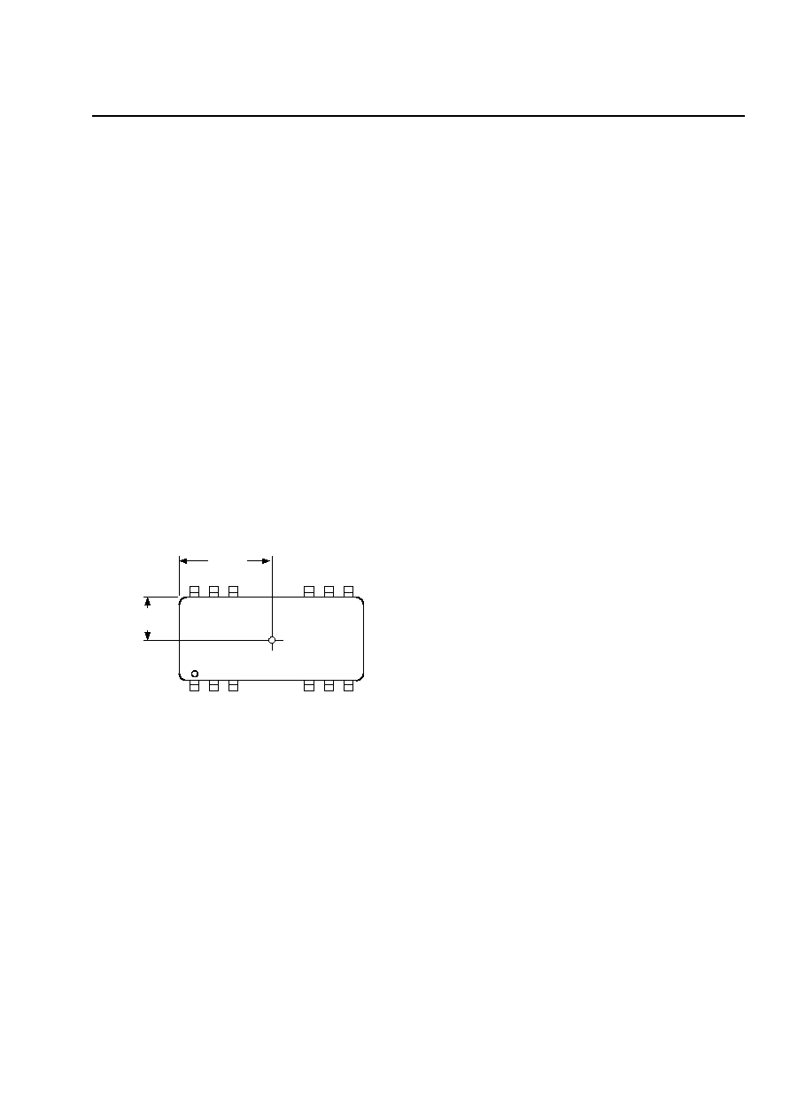
suring the case temperature. The case temperature
(T
C
) should be measured at the position indicated in
Figure 7.
8-1363e
Note: Dimensions are in millimeters and (inches). Pin locations are
for reference only.
Figure 7. SMLW Case Temperature
Measurement Location
Note that the view in Figure 7 is of the surface of the
module. The temperature at this location should not
exceed the maximum case temperature indicated on
the derating curves. The output power of the module
should not exceed the rated power for the module as
listed in the Ordering Information table.
Heat Transfer Characteristics
Increasing airflow over the module enhances the heat
transfer via convection. Figure 8 shows the maximum
power that can be dissipated by the module without
exceeding the maximum case temperature versus local
ambient temperature (T
A
) for natural convection
through 3.0 ms
≠1
(600 ft./min.).
Systems in which these power modules are used typi-
cally generate natural convection airflow rates of
0.25 ms
≠1
(50 ft./min.) due to other heat-dissipating
components in the system. Therefore, the natural con-
vection condition represents airflow rates of approxi-
mately 0.25 ms
≠1
(50 ft./min.). Use of Figure 8 is shown
in the following example.
Example
What is the minimum airflow necessary for an
SMLW010A operating at V
I
= 48 V, an output current of
1.6 A, and a maximum ambient temperature of 86 ∞C?
Solution
Given: V
I
= 48 V, I
O
= 1.6 A (I
O, max
), T
A
= 86 ∞C
Determine P
D
(Figure 9): P
D
= 2.1 W
Determine airflow (Figure 8): v = 1 ms
≠1
(200 ft./min.)
SMLW010A
DC-DC Power Module
IN:DC 36-75V, 0.6A OUT:DC 5V, 2A
1
24 (0.94)
11
(0.45)

10
10
Tyco Electronics Corp.
Data Sheet
January 2002
Power Modules: 36 Vdc to 75 Vdc Input; 10 W
SMLW010 Single-Output Low-Profile
Thermal Considerations
(continued)
Heat Transfer Characteristics
(continued)
8-2793a
Figure 8. SMLW010A and SMLW010G Forced
Convection Power Derating; Either
Orientation
8-2790
Figure 9. SMLW010A Typical Power Dissipation
vs. Normalized Output Current at
T
A
= 25 ∞C
Module Derating
The derating curves in Figure 8 were derived by mea-
surements obtained in an experimental apparatus
shown in Figure 10. Note that the module and the
printed-wiring board (PWB) that it is mounted on are
both vertically oriented. The passage has a rectangular
cross section.
8-1126e
Note: Dimensions are in millimeters and (inches).
Figure 10. Experimental Test Setup
Surface-Mount Power Module Solder
Reflow Recommendation
The SMLW010 Single-Output, Low-Profile, PCB Mount
Power Modules are constructed with SMT (surface-
mount technology) components and assembly guide-
lines. Such large mass/low thermal resistance devices
heat up slower than typical SMT components. It is rec-
ommended that the customer review data sheets in
order to customize the solder reflow profile for applica-
tion board assembly.
It is recommended that a reflow profile must be charac-
terized for the module on the application board assem-
bly. The solder paste type, component, and board
thermal sensitivity must be considered in order to form
the desired fused solder fillet. The power module leads
are plated with tin (Sn) solder to prevent corrosion and
ensure good solderability. Typically, the eutectic solder
melts at 183 ∞C, wets the land, and subsequently wicks
the device lead. Sufficient time must be allocated to
fuse the plating on the lead and ensure a reliable sol-
der joint.
55
70
65
80
85
95
90
100
0.0
3.0
MAX AMBIENT TEMPERATURE, T
A
(
∞C)
2.0
1.5
2.5
105 110
50
PO
WE
R
D
I
SS
I
P
AT
I
O
N
,
P
D
(W
)
1.0
0.5
3.5
60
75
3.0 ms
-1
(600 ft./min.)
2.0 ms
-1
(400 ft./min.)
1.5 ms
-1
(300 ft./min.)
1.0 ms
-1
(200 ft./min.)
NATURAL CONVECTION
MAX CASE TEMPERATURE
0.2
0.4
1.2
1.4
1.6
1.8
0.0
2.5
OUTPUT CURRENT, I
O
(A)
1.5
1.0
2.0
2.0
0.0
3.0
0.5
0.8
1.0
0.6
P
O
W
E
R
D
I
S
S
IP
A
T
IO
N
,
P
D
(W
)
V
I
= 75 V
V
I
= 60 V
V
I
= 48 V
V
I
= 36 V
AIR VELOCITY
AND AMBIENT
TEMPERATURE
MEASURED
BELOW THE
MODULE
AIRFLOW
13 (0.5)
FACING PWB
MODULE
76 (3.0)
PWB
25 (1.0)

Tyco Electronics Corp.
11
Data Sheet
January 2002
Power Modules: 36 Vdc to 75 Vdc Input; 10 W
SMLW010 Single-Output Low-Profile
Surface-Mount Power Module Solder Reflow Recommendation
(continued)
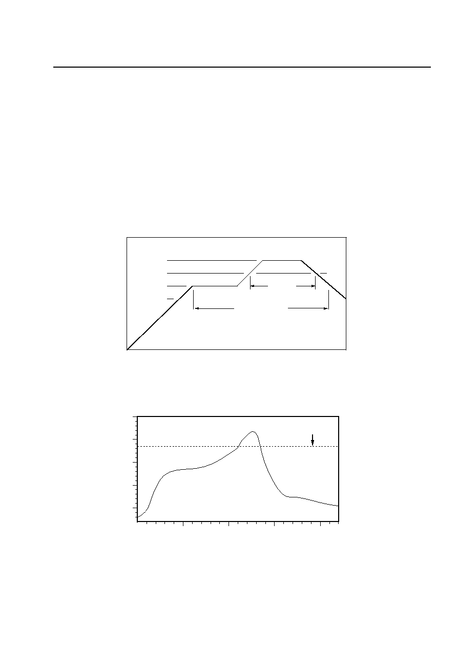
There are several types of SMT reflow technologies currently used in the industry. These surface-mount power
modules can be adequately soldered using natural convection, IR (radiant infrared), convection/IR, or forced con-
vection technologies. The surface-mount power module solder reflow profile is established by accurately measur-
ing the module gull-wing lead surface temperature.
The maximum oven temperature and conveyor speed should prevent the lead temperature from exceeding the
maximum thermal profile limits as shown in Figure 11. The lead temperature during a typical reflow profile is shown
in Figure 12. Failure to observe these maximum lead temperatures and duration may result in permanent damage
to the power module.
Relative temperatures of the module gull-wing leads vary according to many factors, including surrounding compo-
nents, internal paths, and connecting paths. Typically, pin 1 is a good choice for a conservative measurement since
it is usually connected to heavy paths for current conduction which also tend to heat the lead faster. These vari-
ables make it difficult to compare various types of surface-mount modules; however, the unit has been found to be
more robust during temperature profiles compared with other SMT modules available in the industry.
8-2275
Figure 11. Maximum Thermal Profile Limits
8-2274a
Figure 12. Typical Reflow Soldering Profile
4 ∞C/s MAX
90 s MAX
6 MINUTES MAX
230 ∞C MAX
183 ∞C
150 ∞C
120 ∞C
TIME (s)
GULL-WING LEAD
TEMPERA
TURE (
∞
C)
(PEAK)
2:30
5:00
7:30
10:00
MELTING POINT
(60/40 SOLDER)
250
200
150
100
50
TIME (min.)
GULL-WING LEAD
TEMPERA
TURE (
∞
C)

12
Tyco Electronics Corp.
Data Sheet
January 2002
Power Modules: 36 Vdc to 75 Vdc Input; 10 W
SMLW010 Single-Output Low-Profile
Packaging Information
Vacuum Formed Trays
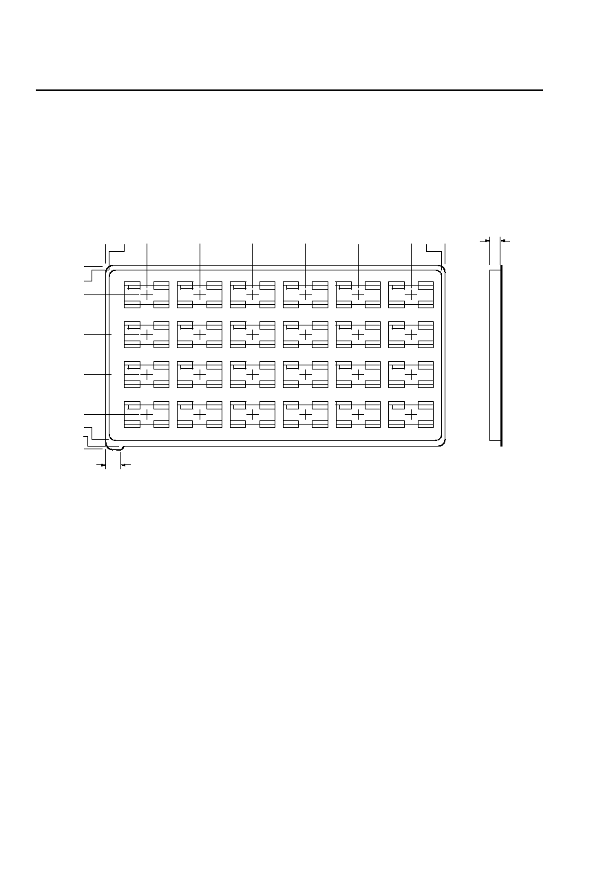
The SMLW010 Single-Output, Low-Profile, PCB Mount Power Modules are delivered in plastic vacuum formed
trays (see Figure 13) that allow automated placement of the modules via a surface-mount pick and place machine.
8-2792
Note: Dimensions are in millimeters and (inches).
Figure 13. Vacuum Formed Tray
Specifications:
Material: PVC (ESD protected)
Capacity: 24 pieces/tray
Weight: 90 g (3.2 oz.)
0.00
3 (0.11)
45 (1.78)
105 (4.14)
165 (6.50)
285 (11.22)
345 (13.58)
378 (14.89)
381 (15.00)
12
(0.47)
216 (8.50)
212 (8.33)
184 (7.25)
90 (3.55)
43 (1.70)
12 (0.48)
4 (0.16)
0.00
19
(0.75)
848276036
225 (8.86)
137 (5.40)

Tyco Electronics Corp.
13
Data Sheet
January 2002
Power Modules: 36 Vdc to 75 Vdc Input; 10 W
SMLW010 Single-Output Low-Profile
Outline Diagram
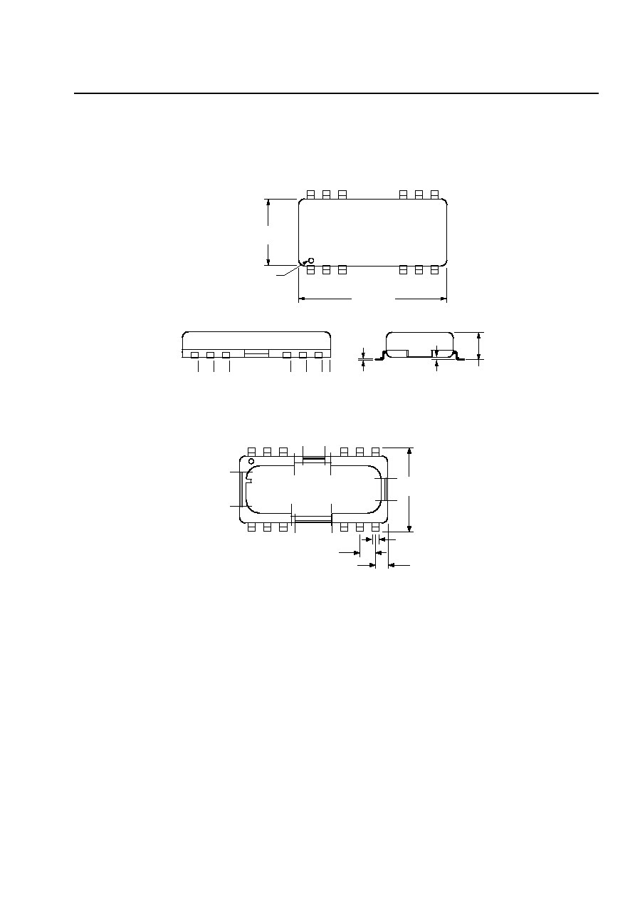
Dimensions are in millimeters and (inches). See next page for pin descriptions.
Tolerances: x.x ± 0.5 mm (0.020 in.); x.xx ± 0.38 mm (0.015 in.).
Top View
Side View
Bottom View
8-2791
22.6
(0.89)
PIN 1 MARK
47.8 (1.88)
SMLW010A
DC-DC Power Module
IN:DC 36-75V, 0.6A OUT:DC 5V, 2A
1
0.30 ± 0.1
(0.012 ± 0.004)
0.25
(0.010)
8.5
(0.335)
MAX
42.60 (1.677)
37.62 (1.481)
32.61 (1.284)
12.60 (0.496)
7.59 (0.299)
2.62 (0.103)
0 (0.000)
28.4
(1.12)
2.54
(0.100)
5.0
(0.197)
3.89
(0.153)
1
2
3
6
5
4
7
8
9
10
11
12

14
Tyco Electronics Corp.
Data Sheet
January 2002
Power Modules: 36 Vdc to 75 Vdc Input; 10 W
SMLW010 Single-Output Low-Profile
Recommended Hole Pattern
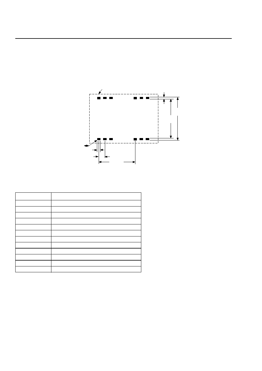
Component-side footprint. Dimensions are in millimeters and (inches).
Tolerances: x.x ± 0.5 mm (0.020 in.); x.xx ± 0.38 mm (0.015 in.).
CAUTION: Care must be taken to ensure the board in the periphery of the footprint is flat.
8-1507d
* The recommended solder paste volume is 2.8 cubic mm (170,000 cubic mils/pin). See Design Considerations section.
NC may be used for internal module connections and should not be connected by the customer.
Pin
SMLW Function
1
V
O
(+)
2
V
O
(≠)
3
TRIM
4
NC
5
NC
6
NC
7
NC
8
ON/OFF
9
SYNC (optional)
10
NC
11
V
I
(≠)
12
V
I
(+)
30.0
(1.181)
3.3
(0.13)
5.0
(0.197)
2.8
(0.110)
FOOTPRINT
PERIPHERY
29.87
(1.176)
24.28
(0.956)
PIN 1 PAD*

Tyco Electronics Corp.
15
Data Sheet
January 2002
Power Modules: 36 Vdc to 75 Vdc Input; 10 W
SMLW010 Single-Output Low-Profile
Ordering Information
Table 6. Device Codes
Optional features may be ordered using the device code suffixes shown below. The feature suffixes are listed
numerically in descending order. Please contact your Tyco Electronics' Account Manager or Field Application Engi-
neer for pricing and availability.
Table 7. Device Options
* Custom option. May not be available on all codes.
Input Voltage
Output Voltage
Output Current
Output Power
Device Code
Comcode
48 V
2.5 V
3 A
7.5 W
SMLW010G
108609744
48 V
5 V
2 A
10 W
SMLW010A
108520396
Option
Device Code Suffix
Synchronization*
3

Data Sheet
January 2002
Power Modules: 36 Vdc to 75 Vdc Input; 10 W
SMLW010 Single-Output Low-Profile
Printed on
Recycled Paper
World Wide Headquarters
Tyco Electronics Power Systems, Inc.
3000 Skyline Drive, Mesquite, TX 75149, USA
+1-800-526-7819 FAX: +1-888-315-5182
(Outside U.S.A.: +1-972-284-2626, FAX: +1-972-284-2900)
www.power.tycoelectronics.com
e-mail: techsupport1@tycoelectronics.com
Tyco Electronics Corporation reserves the right to make changes to the product(s) or information contained herein without notice. No liability is assumed as a result of their use or application.
No rights under any patent accompany the sale of any such product(s) or information.
© 2001 Tyco Electronics Power Systems, Inc. (Mesquite, Texas) All International Rights Reserved.
Printed in U.S.A.
January 2002
DS00-089EPS (Replaces DS99-282EPS)
Europe, Middle-East and Africa Headquarters
Tyco Electronics (UK) Ltd
Tel: +44 (0) 1344 469 300, Fax: +44 (0) 1344 469 301
Central America-Latin America Headquarters
Tyco Electronics Power Systems
Tel: +54 11 4316 2866, Fax: +54 11 4312 9508
Asia-Pacific Headquarters
Tyco Electronics Singapore Pte Ltd
Tel: +65 482 0311, Fax: 65 480 9299
