 | –≠–ª–µ–∫—Ç—Ä–æ–Ω–Ω—ã–π –∫–æ–º–ø–æ–Ω–µ–Ω—Ç: SW10-0313 | –°–∫–∞—á–∞—Ç—å:  PDF PDF  ZIP ZIP |
Matched GaAs SPDT Switch, DC - 3
GHz with TTL/CMOS Control Input
SW10
-
0313
CR-9
V 4.00
Features
n
Integral TTL Driver
n
Low DC Power Consumption
n
Surface Mount Package
n
Low Cost/High Performance
n
50 Ohm Nominal Impedance
Description
M/A-COM's SW10-0313 is a GaAs FET SPDT absorptive
switch with integral silicon ASIC driver. Packaged in a
16-lead ceramic surface mount package, this device offers
excellent performance and repeatability from DC to 3 GHz
while maintaining low power consumption. The
SW10-0313 is ideally suited for use where fast speed, low
power consumption and broadband applications are
required.
Electrical Specifications
1,2
T
A
= +25∞C
Parameter
Test Conditions
Frequency
Units
Min
Typ
Max
Insertion Loss
--
DC - 3000 MHz
DC - 2000 MHz
DC - 1000 MHz
DC - 500 MHz
dB
dB
dB
dB
--
--
--
--
0.8
0.7
0.7
0.6
1.2
1.1
0.9
0.8
VSWR
--
DC - 3000 MHz
DC - 2000 MHz
DC - 1000 MHz
DC - 500 MHz
Ratio
Ratio
Ratio
Ratio
--
--
--
--
1.2:1
1.2:1
1.2:1
1.1:1
1.4:1
1.35:1
1.35:1
1.3:1
Isolation
--
DC - 3000 MHz
DC - 2000 MHz
DC - 1000 MHz
DC - 500 MHz
dB
dB
dB
dB
35
45
45
50
40
50
50
55
--
--
--
--
Trise, Tfall
10% to 90%
--
ns
--
50
--
Ton, Toff
1.3V CTL to 90% / 10%
--
ns
--
150
--
Transients
In-Band
--
mV
--
50
--
1 dB Compression
Input Power
0.05 GHz
0.5 GHz to 3 GHz
dBm
dBm
--
--
+25
+30
--
--
IP2
Two-Tone Input Power up to +5 dBm
0.05 GHz
0.5 GHz to 3 GHz
dBm
dBm
--
--
+60
+65
--
--
IP3
Two-Tone Input Power up to +5 dBm
0.05 GHz
0.5 GHz to 3 GHz
dBm
dBm
--
--
+40
+46
--
--
Vin Low
0V to 0.8V
--
µA
--
--
1
Vin High
2.0V to 5.0V
--
µA
--
--
1
1. All specifications apply when operated with bias voltages of +5V for Vcc and ≠5V for Vee.
2. When DC blocks are used, a 10K ohm return to GND is required on the RFC port.
Matched GaAs SPDT Switch, DC - 3 GHz with TTL/CMOS Control Input
SW10-0313
Specifications subject to change without notice.
n
North America: Tel. (800) 366-2266
n
Asia/Pacific: Tel.+81-44-844-8296, Fax +81-44-844-8298
n
Europe: Tel. +44 (1344) 869 595, Fax+44 (1344) 300 020
Visit www.macom.com for additional data sheets and product information.
V 4.00
2
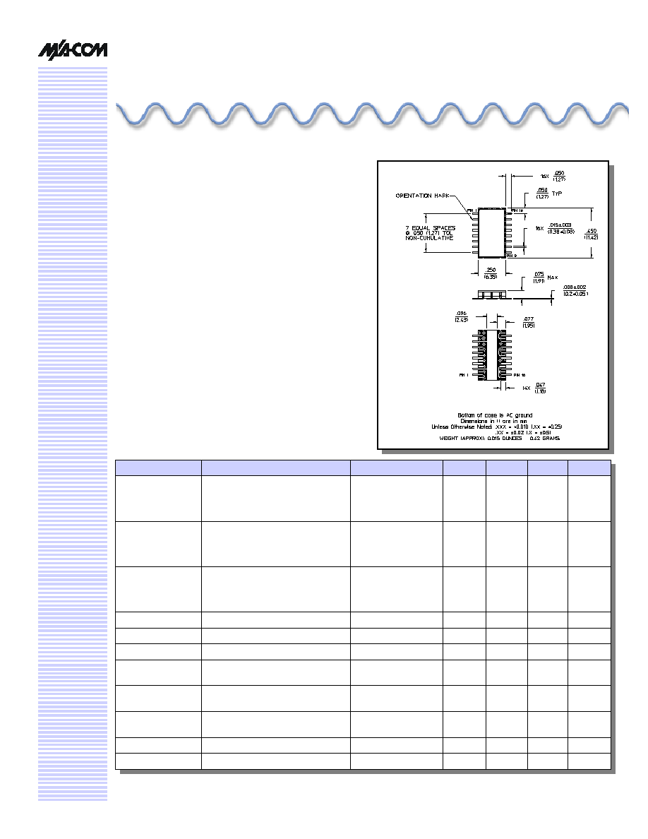
Pin Configuration
Pin No.
Function
Pin No.
Function
1
Vee
9
RFC
2
GND
10
GND
3
GND
11
GND
4
GND
12
RF1
5
RF2
13
GND
6
GND
14
GND
7
GND
15
Vcc
8
GND
16
C1
Absolute Maximum Ratings
3
3. Operation of this device above any one of these parameters
may cause permanent damage.
4. Standard CMOS TTL interface, latch-up will occur if logic
signal is applied prior to power supply.
Parameter
Absolute Maximum
Max Input Power
50 MHz
500 - 2000 MHz
+27 dBm
+34 dBm
Supply Voltages
Vcc
Vee
+5.5V
-8.5V
Control Voltage
4
-0.5V, to Vcc +0.5V
Operating Temperature
-40∞C to +125∞C
Storage Temperature
-65∞C to +150∞C
Truth Table
Condition of Switch
RF Common to Each RF Port
RF1
RF2
LO
On
Off
HIGH
Off
On
C1
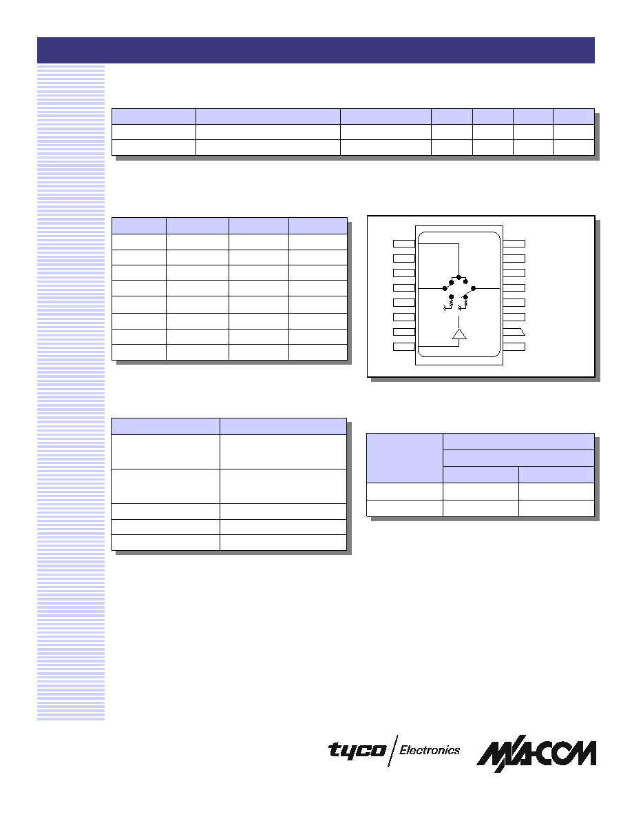
Pin Configuration (Top View)
RFC
GND
GND
RF1
GND
GND
GND
GND
GND
RF2
GND
GND
GND Orientation Mark
Vee
Vcc
C1
Electrical Specifications: T
A
= +25∞C
Parameter
Test Conditions
Frequency
Units
Min
Typ
Max
Vcc
+5.0V ± 10%
--
mA
--
--
1
Vee
-5.0V to -8.0V
--
mA
--
--
1
Matched GaAs SPDT Switch, DC - 3 GHz with TTL/CMOS Control Input
SW10-0313
Specifications subject to change without notice.
n
North America: Tel. (800) 366-2266
n
Asia/Pacific: Tel.+81-44-844-8296, Fax +81-44-844-8298
n
Europe: Tel. +44 (1344) 869 595, Fax+44 (1344) 300 020
Visit www.macom.com for additional data sheets and product information.
V 4.00
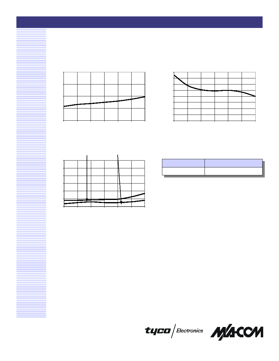
Typical Performance Curves
Isolation vs. Frequency
Insertion Loss vs. Frequency
VSWR vs. Frequency
3
Ordering Information
Part Number
Package
SW10-0313
CR-9
0.00
0.50
1.00
1.50
2.00
0.0
0.5
1.0
1.5
2.0
2.5
3
Frequency (GHz)
Loss (dB)
0
10
20
30
40
50
60
70
80
0.0
0.5
1.0
1.5
2.0
2.5
3
Frequency (GHz)
Isolation dB
1.00
1.20
1.40
1.60
1.80
2.00
2.20
0.0
0.5
1.0
1.5
2.0
2.5
3
Frequency (GHz)
VSWR
VSWR (On)
VSWR (Off)