V 2.00
High Power GaAs SPDT Switch
DC - 3 GHz
SW-106, SW-276
Features
q
+39 dBm Typ. 1 dB Compression Point,
-8V Control
q
+65 dBm Typ. 3rd Order Intercept, -8V Control
q
Insertion Loss of 0.4 dB Typical
q
Low Power Consumption
q
Fast Switching Speed
Guaranteed Specifications
1
(≠55∞C to +85∞C)
Frequency Range
DC - 3.0 GHz
SW-106
SW-276
Insertion Loss
DC - 0.5 GHz
0.5 dB
0.4 dB Max
DC - 1.0 GHz
0.6 dB
0.5 dB Max
DC - 2.0 GHz
0.8 dB
0.7 dB Max
DC - 3.0 GHz
1.2 dB
1.0 dB Max
Isolation
DC - 0.5 GHz
34 dB
37 dB Min
DC - 1.0 GHz
32 dB
31 dB Min
DC - 2.0 GHz
20 dB
24 dB Min
DC - 3.0 GHz
15 dB
19 dB Min
VSWR
DC - 0.5 GHz
1.3:1
1.3:1 Max
DC - 1.0 GHz
1.5:1
1.5:1 Max
DC - 2.0 GHz
1.5:1
1.5:1 Max
DC - 3.0 GHz
1.6:1
1.6:1 Max
Operating Characteristics
2
Impedance
50 Ohms Nominal
Switching Characteristics
Trise, Tfall (10% to 90% )
30 ns Typ
Ton, Toff (50% CTL to 90%/10% RF)
35 ns Typ
Transients (In-Band)
12 mV Typ
Input Power for Compression
0.1 dB
1.0 dB
0.9 GHz
(-5VControl)
+32.5 dBm
+35.5 dBm
Typ
0.9 GHz
(-8V Control)
+35.5 dBm
+39.5 dBm
Typ
Third Order Intercept Point (with two +10 dBm Input Tones)
0.9 GHz
(-5V Control)
+61 dBm Typ
0.9 GHz
(-8V Control)
+65 dBm Typ
Control Voltages
Vin Low
0 to -0.2V @ 20 µA Max
Vin High
-5V @ 50 µA Typ to -10V @ 800 µA Max
1. All specifications apply when operated with bias voltages of 0V for Vin Low
and -5 to -10V for Vin High, and 50 ohm impedance at all RFports, unless
otherwise specified.
2. High power (greater than 1W) handling specifications apply to cold switching
only. For input powers under 1W hot switching can be used.
3. Contact the factory for standard or custom screening requirements.
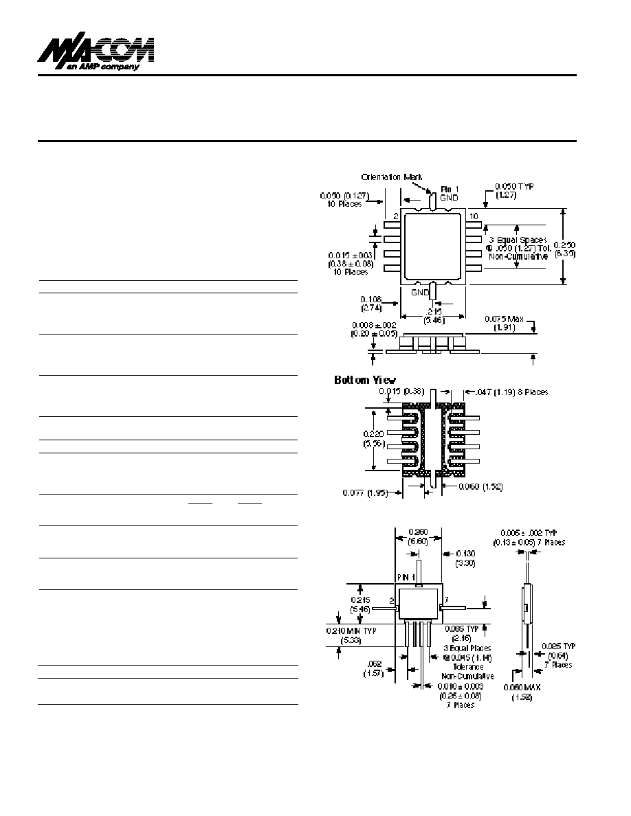
SW-106 (CR-5)
SW-276 (CR-2)
For both switches:
Bottom of Case is AC Ground
Dimension in ( ) are in mm.
Unless Otherwise Noted:
.xxx = ± 0.010 (.xx = ± 0.25)
.xx = ± 0.02 (.x = ± 0.5)
Ordering Information
Part Number
Package
SW-106 PIN
Surface Mount
SW-276 PIN
Ceramic

V 2.00
High Power GaAs SPDT Switch
SW-106, SW-276
Absolute Maximum Ratings
1. Operation of this device above any one of these parameters ma y cause
permanent damage.
2. Tcase = 25∞C, where Tcase is the temperature at the bottom
of the case.
3. Special consideration must be given to the mounting of the switch to
minimize the thermal resistance. The bottom of the case should be
thermally attached to the mounting surface to maintain the junction
temperature under the absolute maximum rating.
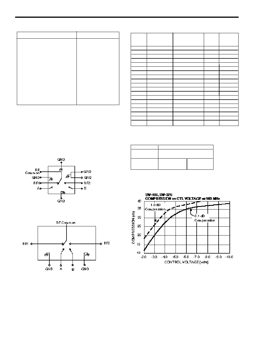
Functional Schematics (Top View)
SW-106
SW-276
Two Tone IP
3
Measurements
Truth Table
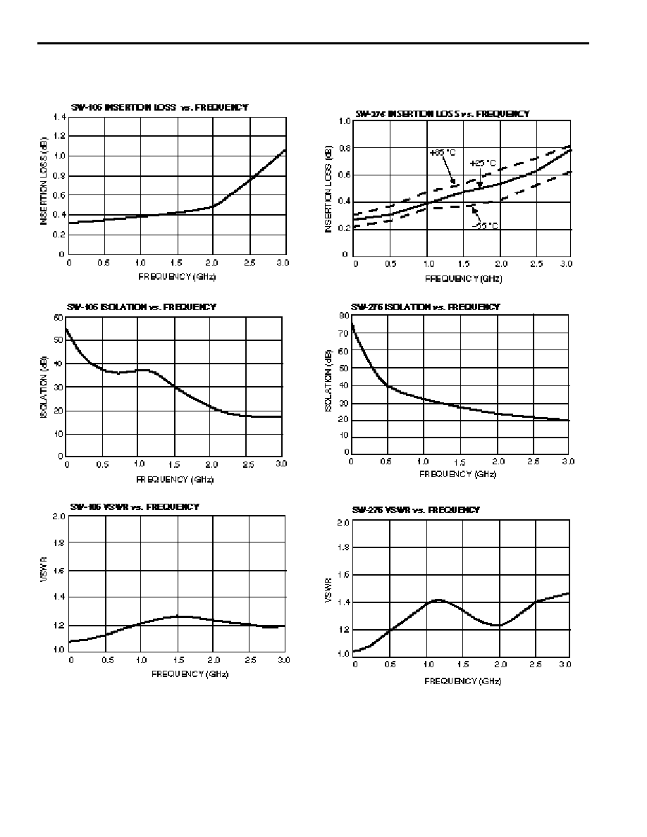
Typical Performance
Parameter
Absolute Maximum
1
Max. Input Power
0.05 GHz
+35 dBm
0.5 - 2.0 GHz
≠5V Control
+36 dBm
≠8V Control
+39 dBm
≠10V Control
+40 dBm
Power Dissipation
2,3
2.0 W
Control Voltage
≠12V, +1V
Operating Temperature
≠55∞C to +125∞C
Storage Temperature
≠65∞C to +150∞C
Maximum Junction Temperature
+175∞C
Thermal Resistance
2
:
jc
+50∞C/W
Control
Condition of Switch
RF Common to Each RF Por t
A
B
RF1
RF2
High Low
On
Off
Low High
Off
On
Input Power
3rd Order
Second
Bias
for each tone
Intermodulation
IP
3
Harmonic
Voltage
(dBm)
Products (dBc)
(dBm)
(dBc)
0, ≠5V
+27
≠34
+44
-61
0, ≠6V
+27
≠49
+51
-61
0, ≠7V
+27
≠64
+59
-63
0, ≠8V
+27
≠65
+59
-63
0, ≠5V
+28
≠30
+43
-58
0, ≠6V
+28
≠41
+48
-58
0, ≠7V
+28
≠52
+54
-57
0, ≠8V
+28
≠60
+58
-57
0, ≠5V
+29
≠28
+43
-54
0, ≠6V
+29
≠34
+46
-54
0, ≠7V
+29
≠44
+51
-54
0, ≠8V
+29
≠52
+55
-54
0, ≠5V
+30
≠26
+43
-52
0, ≠6V
+30
≠32
+46
-51
0, ≠7V
+30
≠38
+49
-51
0, ≠8V
+30
≠44
+52
-51
