High Power GaAs SPDT Switch
DC - 2.5 GHz
SW-277
V3.00
M/A-COM, Inc.
North America:
Tel. (800) 366-2266
s
Asia/Pacific: Tel. +81 3 3263 8761
s
Europe: Tel. +44 (1344) 869 595
Fax (800) 618-8883
Fax +81 3 3263 8769
Fax +44 (1344) 300 020
1
Specifications Subject to Change Without Notice.
Features
∑
Positive Supply and Control Voltages
∑
+36 dBm Typ. 1 dB Compression Point, 8V Supply
∑
+65 dBm Typ. 3rd Order Intercept Point, 8V Supply
∑
Low Insertion Loss: 0.4 dB Typical
∑
Low Power Consumption: 100 µW
∑
Fast Switching Speed
∑
Tape and Reel Packaging Available
1
Description
M/A-COM's SW-277 is a GaAs MMIC SPDT switch in a low cost
SOIC 8-lead surface mount plastic package. The SW-277 is ideally
suited for use where very low power consumption is required.
Typical applications include transmit/receive switching,
switch matrices, and filter banks in systems such as: radio and
cellular equipment, PCM, GPS, fiber optic modules, and other
battery powered radio equipment.
The SW-277 is fabricated with a monolithic GaAs MMIC using a
mature 1-micron process. The process features full chip
passivation for increased performance and reliability.
Electrical Specifications,
T
A
= +25∞C
0∞-8∞
.0075-0.0098
(0.19-0.25)
.1890-.1968
(4.80-5.00)
.0099-0.0196
x 45∞ Chamfer
(0.25-0.50)
.2284-.2440
(5.80-6.20)
PIN 8
Orientation
mark
PIN 1
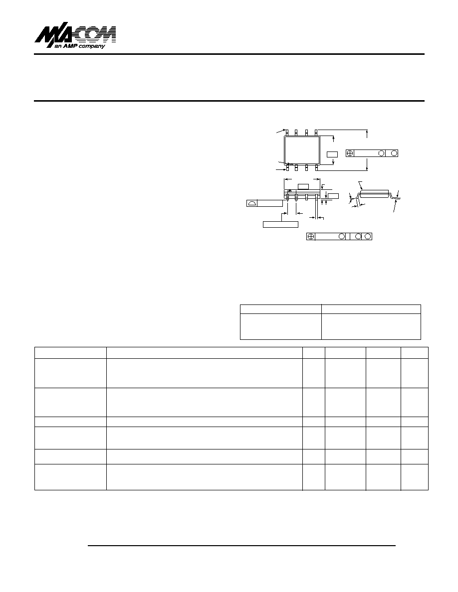
8- Lead SOP outline dimensions
Narrow body .150
(All dimensions per JEDEC No. MS-012-AA, Issue C)
Dimensions in ( ) are in mm.
.1497-.1574
(3.80-4.00)
- B -
- A -
.050(1.27) BSC.
.013-.020 TYP.
(0.33-0.51)
.0040-.0098
(0.10-0.25)
- C -
.0532-.0688
(1.35-1.75)
.016-.050
(0.40-1.27)
.010(0.25) M B M
.010(0.25) M C A M B S
Unless Otherwise Noted: .xxx = ± 0.010 (.xx = ± 0.25)
.xx = ± 0.02 (.x = ±0.5)
.004 (0.10)
SO-8
1. Refer to "Tape and Reel Packaging" Section, or contact factory.
2. All specifications apply when operated with bias voltages of 0V for Vin Low and 5 to 10V for Vin Hi, and 50 Ohm impedance at all RF ports,
unless otherwise specified. High power (greater than 1W) handling specifications apply to cold switches only. For input powers under 1W, hot
switching can be used. The high control voltage must be within +/- 0.2V of the supply voltage. The RF ports must be blocked outside of the pack-
age from ground or any other voltage.
Parameter
Test Conditions
2
Unit
Min.
Typ.
Max
Insertion Loss
DC ≠ 2.0 GHz
dB
0.6
0.8
DC ≠ 1.0 GHz
dB
0.4
0.6
DC ≠ 0.5 GHz
dB
0.35
0.5
DC ≠ 0.1 GHz
dB
0.2
0.4
Isolation
DC ≠ 2.0 GHz
dB
14
16
DC ≠ 1.0 GHz
dB
28
32
DC ≠ 0.5 GHz
dB
35
38
DC ≠ 0.1 GHz
dB
35
38
VSWR
DC ≠ 2.0 GHz
1.2:1
Trise, Tfall
10% to 90% RF, 90% to 10% RF
nS
30
Ton, Toff
50% Control to 90% RF, 50% Control to 10% RF
nS
35
Transients
In Band
mV
12
One dB
Input Power (5V Supply/Control)
0.9 GHz
dBm
33
Compression Point
Input Power (8V Supply/Control)
0.9 GHz
dBm
35.8
3rd Order
Measured Relative (5V Supply/Control)
0.9 GHz
dBm
61
Intercept
to Input Power (8V Supply/Control)
0.9 GHz
dBm
65
(for two-tone input power up to +10 dBm)
Model Number
Package
SW-277 PIN
SOIC 8-Lead Plastic Package
SW-277TR
Forward Tape and Reel
SW-277RTR
Reverse Tape and Reel
Ordering Information
High Power GaAs SPDT Switch
SW-277
V3.00
Absolute Maximum Ratings
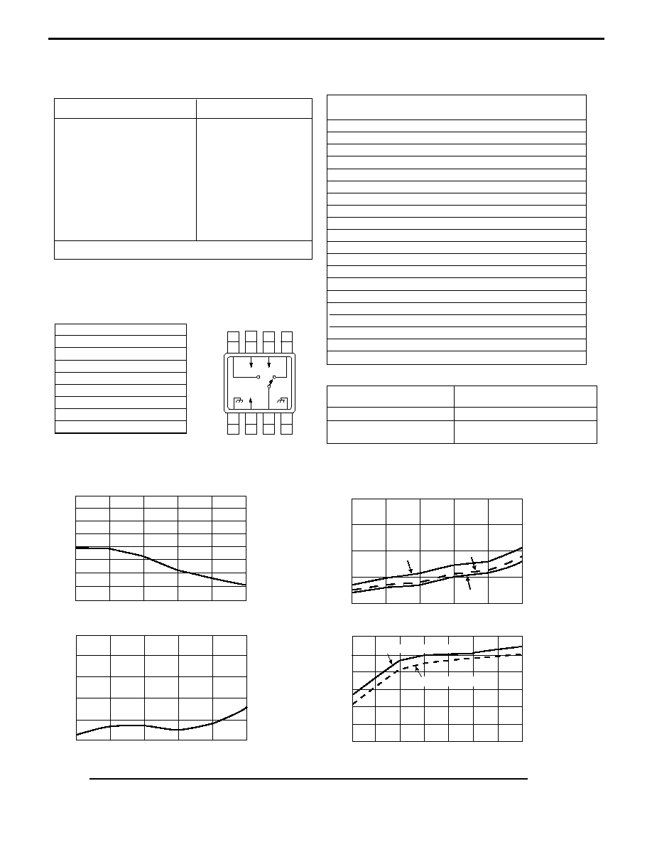
Pin Configuration
Pin No.
Description
1
GND, Thermal Contact
2
+V Supply
3
1
RF Common
4
GND, Thermal Contact
5
1
RF1
6
A
7
B
8
1
RF2
Control Inputs
Condition of Switch
RF Common to Each RF Port
A
B
RF1
RF2
1
0
Off
On
0
1
On
Off
Truth Table
Two Tone IP
3
Measurements
1. Operation of this device above any one of these parameters may cause
permanent damage.
2. Thermal resistance is given for T
A
= 25∞C. T
CASE
is the temperature of
leads 1 and 4.
Parameter Absolute
Maximum
Max. Input Power
0.5 ≠ 2.0 GHz
5V Control and Supply
+37 dBm
8V Control and Supply
+40 dBm
10V Control and Supply
+42 dBm
Power Dissipation
1.0 W
Supply Voltage
-1V, +12V
Control Voltage
-1V, Vsupply + 0.2V
Operating Temperature
-40∞C to +85∞C
Storage Temperature
-65∞C to +150∞C
Thermal Resistance
2
:
jc = 87 ∞C/W
"0" ≠ 0 to +0.2V @ 20 µA max.
"1" ≠ +5V @ 20 µA Typ to 10V @ 500 µA max.
Supply &
Input
3rd Order
Second
Control
Power
Intermodulation
IP3
Harmonic
Voltage
(dBm)
Products (dBc)
(dBm)
(dBc)
0,5V
+27
-32
+43
-74
0,6V
+27
-45
+49.5
-77
0,7V
+27
-58
+56
-79
0,8V
+27
-72
+63
-79
0,10V
+27
-72
+63
-81
0,5V
+28
-30
+43
-69
0,6V
+28
-40
+48
-76
0,7V
+28
-53
+54.5
-78
0,8V
+28
-64
+60
-79
0,10V
+28
-72
+64
-80
0,5V
+29
-28
+43
-59
0,6V
+29
-37
+47.5
-74
0,7V
+29
-49
+53.5
-75
0,8V
+29
-50
+54
-75
0,10V
+29
-50
+54
-75
0,5V
+30
-36
+43
-67
0,6V
+30
-46
+48
-73
0,7V
+30
-50
+53
-75
0,8V
+30
-50
+55
-75
0,10V
+30
-50
+55
-75
8
7
6
5
1
4
3
2
RFC
B
+V
GND
Thermal
Contact
RF2
A
GND
Thermal
Contact
RF1
Functional Schematic
INSERTION LOSS vs. FREQUENCY
FREQUENCY (GHz)
LOSS (dB)
2.0
1.5
1.0
0.5
0
0
0.5
1.0
1.5
2.5
+85∞C
+25∞C
-40∞C
2.0
ISOLATION vs. FREQUENCY
FREQUENCY (GHz)
ISOLATION (dB)
80
60
40
20
0
0
0.5
1.0
1.5
2.5
70
50
30
10
2.0
VSWR vs. FREQUENCY
FREQUENCY (GHz)
VSWR
2.0
1.8
1.6
1.4
1.0
0
0.5
1.0
1.5
2.0
1.2
COMPRESSION vs. CONTROL VOLTAGE (900 MHz)
CONTROL VOLTAGE (Volts)
40
35
30
25
10
3.0
4.0
5.0
6.0
10.0
20
15
7.0
8.0
9.0
1.0 dB Compression
0.1 dB Compression
COMPRESSION (dBm)
Typical Performance
1. External DC blocking capacitors required
on all RF ports.
ISOLATION
VS
FREQUENCY
VSWR
VS
FREQUENCY
INSERTION LOSS
VS
FREQUENCY
COMPRESSION
VS
CONTROL VOLTAGE (900MHz)
M/A-COM, Inc.
North America:
Tel. (800) 366-2266
s
Asia/Pacific: Tel. +81 3 3263 8761
s
Europe: Tel. +44 (1344) 869 595
Fax (800) 618-8883
Fax +81 3 3263 8769
Fax +44 (1344) 300 020
2
Specifications Subject to Change Without Notice.