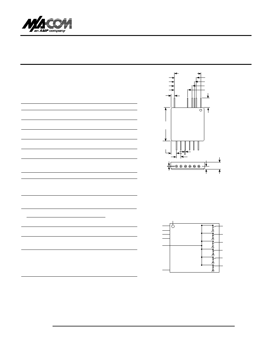
GaAs Matched SP6T Switch
DC - 2 GHz
SW-284
+5VDC
A0
A1
A2
RF6
RF5
RF4
RF3
RF2
RF1
RF Common
-5VDC
Pin Identifier
Functional Schematic (Top View)
0.300 MIN TYP (7.62)
0.150 MAX
0.015 ±.004 12 Places
0.75 Sq
(19.0)
0.125 (3.18)
.010 ±.003 12 Places
.065 TYP (1.65)
0.500 (12.70)
0.450 (11.43)
0.400 (10.16)
0.300 (7.62)
0.075 (1.90)
0.100
5 Places (2.54)
(0.38 ± 0.10)
(3.81)
(0.25 ± 0.08)
0.600 (15.24)
Bottom of Case is AC Ground
Dimensions in ( ) are in mm.
Unless Otherwise Noted: .xxx = ± 0.010 (.xx = ± 0.25)
.xx = ± 0.02 (.x = ± 0.5)
Operating Characteristics
Impedance
50 Ohms Nominal
Switching Characteristics
Trise, Tfall (10% to 90% RF)
3.0 ns Typ
Ton, Toff (50% CTL to 90%/10% RF)
180 ns Typ
Transients (In-Band)
150 mV Typ
Input Power for 1 dB Compression
0.5 ≠ 2.0 GHz
23 dBm Typ
0.05 GHz
21 dBm Typ
Intermodulation Intercept Point (for two-tone input power up to +5 dBm)
Intercept Points
IP2
IP3
0.5 ≠ 2.0 GHz
+60
+45
dBm Typ
0.05 GHz
+53
+35
dBm Typ
Bias Power
-5 VDC @ 2 mA Max
+5 VDC @ 1 mA Max
Control Voltages
Vin Low (0)
0.0 to 1.5V @ 1 µA Max
Vin Hi (1)
3.5 to 5.0V @ 1 µA Max
1. All specifications apply with 50 ohm impedance connected to all RF ports, with
-5 and +5 VDC bias voltages.
2. Contact the factory for standard or custom screening requirements.
Guaranteed Specifications
1
(From -55∞C to +85∞C)
Frequency Range
DC - 2.0 GHz
Insertion Loss
DC ≠ 2.0 GHz
2.8 dB Max
DC ≠ 1.0 GHz
2.0 dB Max
VSWR
DC ≠ 2.0 GHz
.9:1 Max
(RF Common)
DC ≠ 1.0 GHz
1.3:1 Max
VSWR
DC ≠ 2.0 GHz
1.7:1 Max
(RF1-RF6 On)
DC ≠ 1.0 GHz
1.3:1 Max
VSWR
DC ≠ 2.0 GHz
1.3:1 Max
(RF1-RF6 Terminated)
DC ≠ 1.0 GHz
1.3:1 Max
Isolation
DC ≠ 2.0 GHz
28 dB Min
DC ≠ 1.0 GHz
33 dB Min
M/A-COM, Inc.
North America:
Tel. (800) 366-2266
s
Asia/Pacific: Tel. +81 (03) 3226-1671
s
Europe: Tel.
+44 (1344) 869 595
Fax (800) 618-8883
Fax +81 (03) 3226-1451
Fax +44 (1344) 300 020
1
Specifications Subject to Change Without Notice.
V3.00
Ordering Information
Model No.
Package
SW-284 PIN
Flatpack
Features
Low DC Power Consumption
Integral CMOS Decoder/Driver
q
q
Guaranteed Specifications
1
(From -55∞C to +85∞C)
FP-27
GaAs Matched SP6T Switch
SW-284
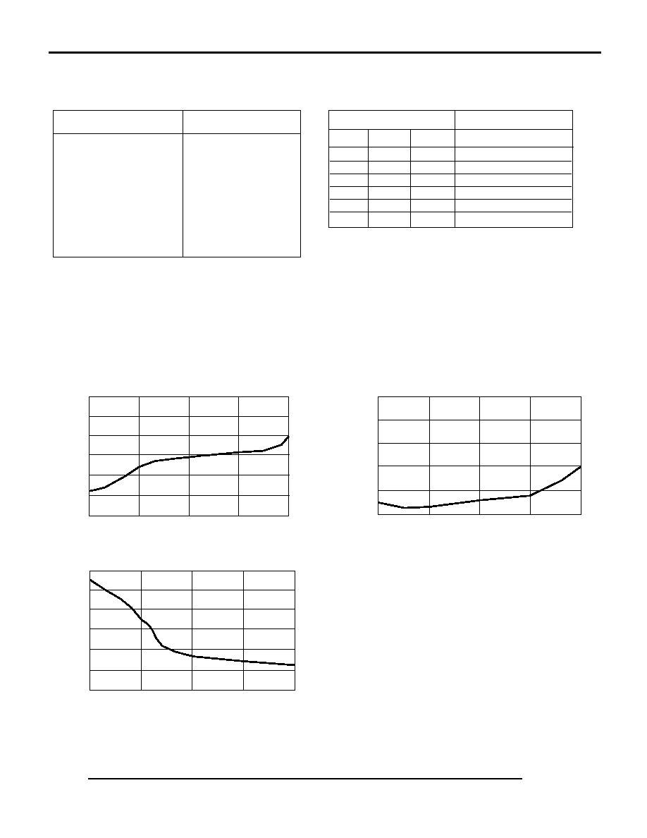
Typical Performance
ISOLATION vs. FREQUENCY
0.5
1.0
1.5
2.0
80
70
60
50
40
30
20
0
FREQUENCY (GHz)
ISOLATION (dB)
VSWR vs. FREQUENCY
2.0
1.8
1.6
1.4
1.2
1.0
0
0.5
1.0
1.5
2.0
FREQUENCY (GHz)
VSWR
Absolute Maximum Ratings
1. Operation of this device above any one of these parameters may
cause permanent damage.
2. When the RF input power is applied to the terminated port,
the absolute maximum is +32 dBm.
Parameter Absolute
Maximum
1
Max. Input Power
0.05 GHz
+27 dBm
0.5 ≠ 2.0 GHz
2
+34 dBm
Bias Voltage
+5V Supply
-0.5 to +7V
-5V Supply
-7V to + 0.5V
Control Voltage
-0.5 to Vcc + 0.5V
Operating Temperature
-55∞C to +125∞C
Storage Temperature
-65∞C to +150∞C
2.0
2.5
2.0
1.5
1.0
0.5
0
0
0.5
1.0
1.5
2.0
INSERTION LOSS vs. FREQUENCY
LOSS (dB)
FREQUENCY (GHz)
Control Input
Condition of Switch
A2
A1
A0
RF Common to
0
0
1
RF1
0
1
0
RF2
0
1
1
RF3
1
0
0
RF4
1
0
1
RF5
1 1
0
RF6
Truth Table
INSERTION LOSS
VS
FREQUENCY
VSWR
VS
FREQUENCY
ISOLATION
VS
FREQUENCY
Typical Performance
Absolute Maximum Ratings
Truth Table
V.3.00
M/A-COM, Inc.
North America:
Tel. (800) 366-2266
s
Asia/Pacific: Tel. +81 (03) 3226-1671
s
Europe: Tel.
+44 (1344) 869 595
Fax (800) 618-8883
Fax +81 (03) 3226-1451
Fax +44 (1344) 300 020
2
Specifications Subject to Change Without Notice.
+27 dBm
+34 dBm
-0.5 to VCC + 0.5V
FREQUENCY (GHz)
-55∞C to +125∞C
-65∞C to +150∞C
-0.5 to +7V
-7V to +0.5V