Features
Very Low Power Consumption: 100 µW
Low Insertion Loss: 0.5 dB
High Isolation: 25 dB up to 2 GHz
Very High Intercept Point: 48 dBm IP3
Nanosecond Switching Speed
Temperature Range: -40∞C to +85∞C
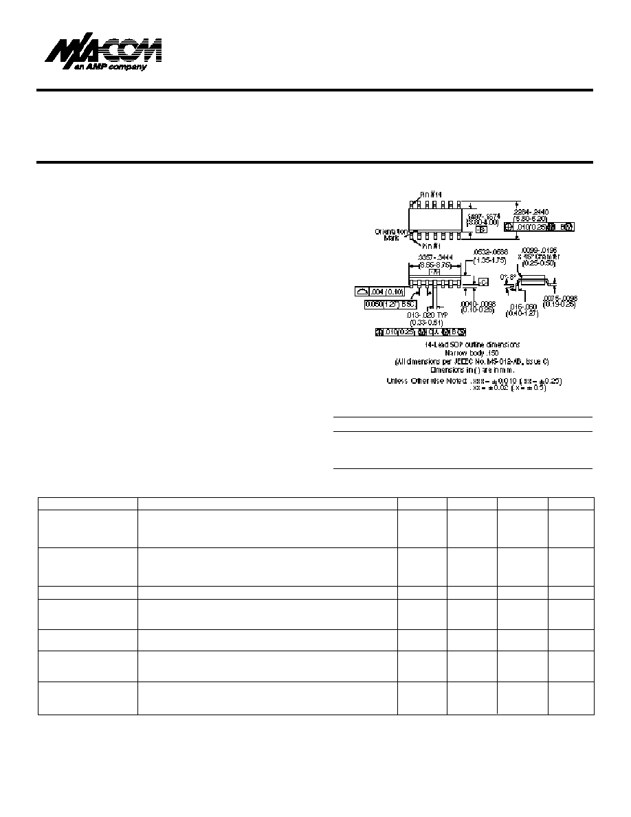
Low Cost SOIC14 Plastic Package
Tape and Reel Packaging Available
1
Description
M/A-COM's SW-289 is a GaAs MMIC DPDT switch in a low cost
SOIC 14-lead surface mount plastic package. The SW-289 is ideally
suited for use where very low power consumption is re q u i re d .
Typical applications include transmit/receive switching, switch
matrices, digital step attenuators, and filter banks in systems such as:
radio and cellular equipment, PCM, GPS, fiber optic modules, and
other battery powered radio equipment.
The SW-289 is fabricated with a monolithic GaAs MMIC using a
m a t u re 1-micron process. The process features full chip passivation
for increased perf o rmance and re l i a b i l i t y .
GaAs DPDT Switch
DC - 2 GHz
S W-289
S O - 1 4
Parameter
Test Conditions
2
Unit
Min.
Typ.
Max
Insertion Loss
DC ≠ 0.1 GHz
dB
0.35
0.5
DC ≠ 0.5 GHz
dB
0.35
0.5
DC ≠ 1.0 GHz
dB
0.4
0.6
DC ≠ 2.0 GHz
dB
0.6
0.8
Isolation
DC ≠ 0.1 GHz
dB
50
56
DC ≠ 0.1 GHz
dB
40
43
DC ≠ 1.0 GHz
dB
32
35
DC ≠ 2.0 GHz
dB
20
23
VSWR
DC ≠ 2.0 GHz
1.3:1
Trise, Tfall
10% to 90% RF, 90% to 10% RF
nS
3
Ton, Toff
50% Control to 90% RF, 50% Control to 10% RF
nS
6
Transients
In Band
mV
15
One dB
Input Power
0.05 GHz
dBm
22
Compression
Input Power
0.5 ≠ 2.0 GHz
dBm
27
Measured Relative
0.05 GHz
dBm
54
IP2
to Input Power
0.5 ≠ 2.0 GHz
dBm
66
(for two-tone input power up to +5 dBm)
Measured Relative
0.05 GHz
dBm
45
IP3
to Input Power
0.5 ≠ 2.0 GHz
dBm
48
(for two-tone input power up to +5 dBm)
Electrical Specifications, TA = +25∞C
1. Refer to "Tape and Reel Packaging" section, or contact factory.
2. All measurements with 0, -5 V control voltages at 1 GHz in a 50
system, unless otherwise specified.
Ordering Information
Part Number
Package
SW-289 PIN
SOIC 14-Lead Plastic Package
SW-289TR
Forward Tape & Reel
SW-289RTR
Reverse Tape & Reel
q
q
q
q
q
q
q
q
V 2.00

V 2.00
GaAs DPDT Switch
S W- 2 8 9
Functional Sch e m a t i c
Truth Ta bl e
Electrical Schematic
Control Input
Condition of Switch
A
B
RF1 TO
RF6 TO
RF2
RF3
RF4
RF 5
1
0
On
Off
On
Off
0
1
Off
On
Off
On
Absolute Maximum Ratings
1
1.Operation of this device above any one of these parameters may cause per-
manent damage.
Parameter
Absolute Maximum
Max. Input Power
0.05 GHz
+27 dBm
0.5 ≠ 2.0 GHz
+34 dBm
Control Voltage
+5 V, -8.5 V
Operating Temperature
-40∞C to +85∞C
Storage Temperature
-65∞C to +150∞C
Pin Configuration
Pin No.
Description
1
RF3
2
GND
3
RFI
4
GND
5
RF2
6
GND
7
A
Pin No.
Description
8
B
9
GND
10
RF4
11
GND
12
RF6
13
GND
14
RF5
Typical Pe r fo r m a n c e
"0" ≠ 0 ≠ -0.2V @ 20 µA max.
"1" ≠ -5V @ 40 µA Typ to -8V @ 900 µA max.
GND