n
North America: Tel. (800) 366-2266, Fax (800) 618-8883
n
Asia/Pacific: Tel.+81-44-844-8296, Fax +81-44-844-8298
n
Europe: Tel. +44 (1344) 869 595, Fax+44 (1344) 300 020
Specifications subject to change without notice.
Visit www.macom.com for additional data sheets and product information.
V 2.0
SW-335
SPDT Switch with Integral CMOS Driver
800 - 2000 MHz
1
Features
Low Cost Plastic SOIC-8 Package
1
I n t e rgral TTL/CMOS Compatible Driver
Matched Input and Output
Low Distortion: > 40 dBm IP3 @ 900 MHz
and > 62 dBm IP2 @ 900 MHz
Low DC Current: < 1.5 mA Typical Per Supply
D e s c r i p t i o n
The SW-335 is a GaAs MMIC matched SPDT with an on-
c h i p TTL/CMOS driver in a low-cost, SOIC 8-lead plastic
package. The SW-335 is ideally suited for use in
TTL/CMOS environment applications where low power
consumption and small size are re q u i red. Typical
applications include switch matrices, filter banks and gen-
eral switching applications, in systems such as celluar,
PCN/PCS, GPS and 900 MHz ISM band applications.
The SW-335 is fabricated with a monolithic GaAs MMIC
using a mature 1-micron process. The process feature s
full passivation for increased perf o rmance and re l i a b i l i t y .
q
q
q
q
q
Electrical Specifications, T
A
= +25∞C, V
DD
= 5.0 V
GG
= -5.0 V
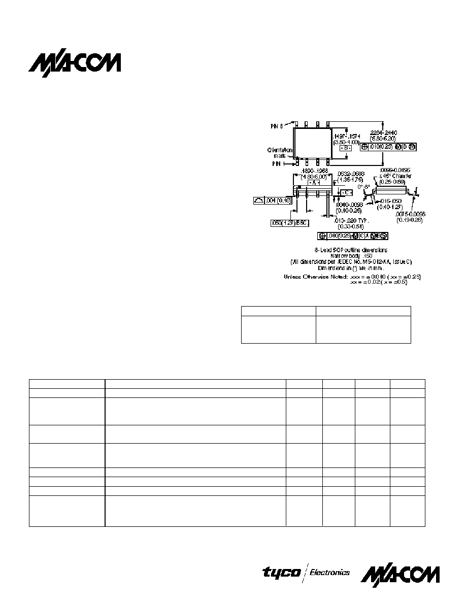
SO-8
Part Number
Package
SW-335 PIN
SOIC 8-Lead Plastic
SW-335TR
Forward Tape & Reel
*
SW-335RTR
Reverse Tape & Reel
*
Ordering Information
1. Available in tape and reel packaging.
2.All measurements are in a 50
system.
3.Replaces SW-329.
4.DC blocks required on RF ports.
*
If specific reel size is required, consult factory for part
number assignment.
Parameter
Test Conditions
Units
Min.
Typ.
Max.
Insertion Loss
800-2000 MHz
dB
0.9
1.1
Isolation
800-1000 MHz
dB
35
45
1000-1500 MHz
dB
35
38
1500-2000 MHz
dB
30
32
VSWR
800-1000 MHz
1.2:1
1.3:1
1000-2000 MHz
1.2:1
1.3:1
Trise, Tfall
10%-90% RF, 90% - 10% RF
nS
75
Ton , Toff
50% Control to 90% RF, 50% Control to 10% RF
nS
200
Transient
In-Band
mV
20
1 dB Compression
900 MHz
dBm
29
Input IP3
2-Tone, 10 dBm (13 dBm total)
900 MHz
dBm
40
45
Input IP2
2-Tone, 10 dBm (13 dBm total)
900 MHz
dBm
62
70
Current
V
DD
@ 5.0 V
mA
1.1
1.5
V
GG
@ -5.0 V
mA
-0.8
-1.5
V
CTL
@ 0 V
µA
-5
-10
V
CTL
@ 5 V
µA
10
20

n
North America: Tel. (800) 366-2266, Fax (800) 618-8883
n
Asia/Pacific: Tel.+81-44-844-8296, Fax +81-44-844-8298
n
Europe: Tel. +44 (1344) 869 595, Fax+44 (1344) 300 020
Specifications subject to change without notice.
Visit www.macom.com for additional data sheets and product information.
V 2.0
SPDT Switch with Integral CMOS Driver, 800-2000 MHz SW-335
2
Parameter
Absolute Maximum
RF Input Power
+31 dBm
Max. Control Voltages
V
DD
+6 VDC
V
GG
-6 VDC
V
CTL
Maximum
+6 VDC
V
CTL
Minimum
-1 VDC
Operating Temperature
-40∞C to +85∞C
Storage Temperature
-65∞C to +150∞C
Control Input
TTL/CMOS
RFC-RF1
RFC-RF2
1
OFF
ON
0
ON
OFF
Absolute Maximum Ratings
1
Truth Table
Functional Schematic
1.Operation of this device outside these limits may cause
permanent damage.
I S O L ATION vs F R E QUENCY OVER T E M P E R AT U R E
Typical Performance
OUTPUT VSWR ("OFF" S TATE) vs FREQU E N C Y
OVER T E M P E R AT U R E
Logic 0 = 0 to 1 V
Logic 1 = 3.5 to 5 V, 10 µA typ.
V
DD
= 5 ±0.5 V @ < 1.5 mA typ.
V
GG
= -5 ±0.25 V @ < 1.5 mA
50
45
40
35
30
0.8
1.0
1.2
1.4
1.6
1.8
2.0
FREQUENCY (GHz)
1.2
0.9
0.6
0.3
0.0
0.8
1.0
1.2
1.4
1.6
1.8
2.0
FREQUENCY (GHz)
I N S E RTION LOSS vs F R E Q. OVER T E M P E R AT U R E
+70∞C
+25∞C
0∞C
1.25
1.20
1.15
1.10
1.05
1.00
0.8
1.0
1.2
1.4
1.6
1.8
2.0
FREQUENCY (GHz)
FREQUENCY (GHz)
OUTPUT VSWR ("ON" S TATE) vs FREQU E N C Y
OVER T E M P E R AT U R E
1.25
1.20
1.15
1.10
1.05
1.00
0.8
1.0
1.2
1.4
1.6
1.8
2.0
INPUT VSWR vs FREQUENCY OVER T E M P E R AT U R E
+70∞C
+25∞C
0∞C
+70∞C
+25∞C
0∞C
+70∞C
+25∞C
0∞C

